
Texas Instruments
TLC272BCD
OP Amps, Buffer Amps ICs


.png?x-oss-process=image/format,webp/resize,p_30)


TLC272BCD Description
TLC272BCD Description
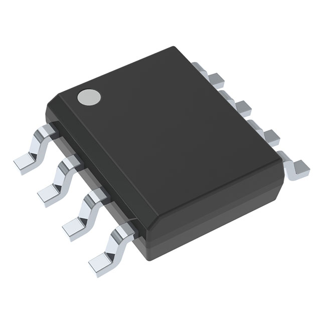
The TLC272BCD from Texas Instruments is a dual-channel CMOS operational amplifier (op-amp) belonging to the LinCMOS™ series. Designed for precision and efficiency, it operates over a 3V to 16V supply range, making it versatile for both low-voltage and moderate-voltage applications. With a 2.2 MHz gain bandwidth product and a 5.3V/µs slew rate, it delivers high-speed performance while maintaining low power consumption (1.9mA per channel). The device features ultra-low input bias current (0.7 pA) and low input offset voltage (290 µV), ensuring accuracy in sensitive analog circuits. Packaged in an 8-SOIC tube, it is RoHS3 compliant and rated for 0°C to 70°C operation, suitable for industrial and consumer electronics.
TLC272BCD Features
- CMOS Technology: Ensures low power consumption and high input impedance.
- Wide Supply Range (3V–16V): Compatible with single or dual-supply configurations.
- Low Input Bias Current (0.7 pA): Ideal for high-impedance sensor interfaces and precision integrators.
- High Slew Rate (5.3V/µs): Supports fast signal processing in data acquisition systems.
- Dual-Channel Design: Space-efficient solution for multi-stage amplification.
- Robust Packaging (8-SOIC): Surface-mount ready with MSL 1 (Unlimited) moisture sensitivity.
TLC272BCD Applications
- Sensor Signal Conditioning: Amplifies low-level signals from thermocouples, strain gauges, or photodiodes.
- Active Filters: Suitable for low-noise, high-precision filter designs due to its low offset voltage.
- Portable Electronics: Ideal for battery-powered devices (e.g., medical instruments, handheld meters) owing to its low current draw.
- Data Acquisition Systems: High slew rate and bandwidth enable accurate analog-to-digital conversion.
- Industrial Control Systems: Reliable performance in motor control or process monitoring applications.
Conclusion of TLC272BCD
The TLC272BCD stands out for its low-power CMOS architecture, wide voltage range, and precision performance, making it a superior choice over traditional bipolar op-amps in noise-sensitive or power-constrained designs. Its dual-channel integration and industrial-grade reliability cater to diverse applications, from portable gadgets to industrial automation. While classified as Last Time Buy, its REACH unaffected status ensures continued compliance for legacy systems. Engineers seeking a balance of speed, accuracy, and efficiency will find this op-amp a compelling solution.
Tech Specifications
TLC272BCD Documents
Download datasheets and manufacturer documentation for TLC272BCD
 TLC272/A/B/Y, TLC277
  EOL NOTICE 17/Feb/2023 EOL PDN20230217005.3A 23/Feb/2023
  Mult Devices Font 21/Apr/2018 Design 25/Feb/2022
 Shopping Guide


.png?x-oss-process=image/format,webp/resize,h_32)


