

Texas Instruments
TLC272CPW
OP Amps, Buffer Amps ICs

Not available to buy online? Want the lower wholesale price? Please Send RFQ to get best price, we will respond immediately


.png?x-oss-process=image/format,webp/resize,p_30)


TLC272CPW Description
TLC272CPW Description
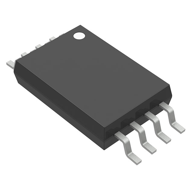
The TLC272CPW from Texas Instruments is a dual-channel CMOS operational amplifier (op-amp) from the LinCMOS™ series, designed for precision analog applications. Packaged in an 8-pin TSSOP (Tube), it operates over a 3V to 16V supply range, making it versatile for both low-voltage and industrial-level designs. With a 2.2 MHz gain bandwidth product (GBW) and 5.3V/µs slew rate, it balances speed and power efficiency, drawing only 1.9mA per channel. Its ultra-low input bias current (0.7 pA) and 1.1 mV input offset voltage ensure high accuracy in signal conditioning.
TLC272CPW Features
- Low Power Consumption: Ideal for battery-powered devices, with 1.9mA/channel supply current.
- Wide Supply Range: Supports 3V to 16V, accommodating diverse power environments.
- High Precision: 0.7 pA input bias current and 1.1 mV offset voltage minimize errors in sensitive circuits.
- Fast Response: 5.3V/µs slew rate and 2.2 MHz GBW enable efficient signal processing.
- Robust Packaging: 8-TSSOP surface-mount package ensures compact PCB integration.
- Compliance: ROHS3 Compliant and REACH Unaffected, meeting environmental standards.
TLC272CPW Applications
- Sensor Interfaces: Ideal for amplifying low-level signals from thermocouples, strain gauges, or photodiodes due to its low input bias current.
- Portable Electronics: Suits wearables and IoT devices with its low power draw and wide voltage range.
- Active Filters & Signal Conditioning: The 2.2 MHz GBW supports audio and instrumentation filtering.
- Industrial Control Systems: Operates reliably in 0°C to 70°C environments, suitable for factory automation.
- Medical Devices: Precision and low noise make it apt for ECG amplifiers and biosensors.
Conclusion of TLC272CPW
The TLC272CPW stands out for its low-power precision, wide voltage flexibility, and CMOS-based reliability, making it a top choice for analog front-ends, portable systems, and industrial controls. While marked as Last Time Buy, its performance metrics—such as near-zero input bias current and fast slew rate—ensure it remains a competitive solution for legacy and new designs requiring high accuracy and efficiency. Engineers should consider this op-amp for cost-sensitive, precision-critical applications where Texas Instruments' proven LinCMOS™ technology delivers consistent results.
Tech Specifications
TLC272CPW Documents
Download datasheets and manufacturer documentation for TLC272CPW
TLC272/A/B/Y, TLC277 EOL NOTICE 17/Feb/2023 EOL PDN20230217005.3A 23/Feb/2023 Design 22/Feb/2022 Related Parts


Shopping Guide


.png?x-oss-process=image/format,webp/resize,h_32)


©2025 ERSA Electronics Corporation.