
Texas Instruments
TLC27L7CD
OP Amps, Buffer Amps ICs


.png?x-oss-process=image/format,webp/resize,p_30)


TLC27L7CD Description
TLC27L7CD Description
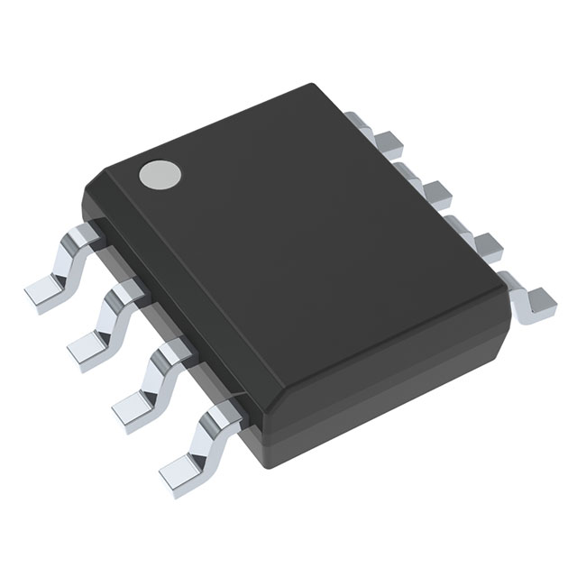
The TLC27L7CD is a dual CMOS operational amplifier from Texas Instruments, designed for a wide range of applications requiring low power consumption and high performance. This IC features a supply voltage range of 3 V to 16 V, making it suitable for both low-voltage and higher voltage systems. With a gain bandwidth product of 110 kHz and a slew rate of 0.03 V/µs, the TLC27L7CD offers reliable performance in signal processing and amplification tasks. The device is housed in an 8-pin SOIC package, ensuring ease of integration into surface-mount designs.
TLC27L7CD Features
- Low Power Consumption: The TLC27L7CD operates with a supply current of only 20 µA per channel, making it ideal for battery-powered and low-power applications.
- High Input Impedance: With an input bias current of just 0.6 pA, this op-amp minimizes loading effects on sensitive input sources.
- Low Input Offset Voltage: The 1.1V m input offset voltage ensures high accuracy in signal amplification and processing.
- Wide Supply Voltage Range: The 3 V to 16 V supply voltage range provides flexibility in various power supply configurations.
- High Output Current Capability: Each channel can drive up to 30 mA, allowing the TLC27L7CD to drive moderate loads directly.
- CMOS Technology: The CMOS design offers high input impedance and low power consumption, enhancing overall system efficiency.
- Surface Mount Packaging: The 8-pin SOIC package is suitable for automated assembly processes, ensuring high reliability and ease of integration.
- Compliance and Reliability: The TLC27L7CD is REACH unaffected and RoHS3 compliant, ensuring environmental safety and regulatory compliance. It also has a moisture sensitivity level (MSL) of 1, making it suitable for unlimited storage.
TLC27L7CD Applications
The TLC27L7CD is well-suited for a variety of applications where low power consumption and high performance are critical. Some specific use cases include:
- Battery-Powered Devices: The low power consumption makes it ideal for portable electronics and battery-operated systems.
- Signal Conditioning: The high input impedance and low offset voltage are beneficial for precision signal conditioning in sensors and transducers.
- Analog Signal Processing: The wide supply voltage range and CMOS technology ensure reliable performance in analog signal processing applications.
- Consumer Electronics: The TLC27L7CD can be used in consumer electronics for amplifying audio signals or processing analog data.
- Industrial Control Systems: The robustness and compliance with environmental standards make it suitable for industrial applications where reliability and safety are paramount.
Conclusion of TLC27L7CD
The TLC27L7CD from Texas Instruments is a versatile dual CMOS operational amplifier that offers a combination of low power consumption, high input impedance, and wide supply voltage range. Its unique features, such as low input bias current and low input offset voltage, make it an excellent choice for precision signal processing and low-power applications. The surface-mount packaging and compliance with environmental standards ensure ease of integration and regulatory compliance. Whether used in portable devices, consumer electronics, or industrial control systems, the TLC27L7CD provides reliable performance and high efficiency, making it a valuable component in modern electronic designs.
Tech Specifications
TLC27L7CD Documents
Download datasheets and manufacturer documentation for TLC27L7CD
 TLC27L2(A, B), TLC27L7 Datasheet
  EOL 22/May/2023
  TLC27L2(A, B), TLC27L7 Datasheet
  Mult Devices Font 21/Apr/2018 Design 25/Feb/2022
 Shopping Guide


.png?x-oss-process=image/format,webp/resize,h_32)


