
Texas Instruments
TLC4502AMD
OP Amps, Buffer Amps ICs


.png?x-oss-process=image/format,webp/resize,p_30)


TLC4502AMD Description
TLC4502AMD Description
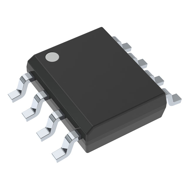
The TLC4502AMD is a high-performance CMOS operational amplifier from Texas Instruments, designed for a wide range of linear amplifier applications. This dual-channel amplifier features a supply voltage range of 4 V to 6 V, making it suitable for low-voltage systems. Each channel can deliver up to 50 mA of output current, ensuring robust performance in various electronic circuits. The TLC4502AMD boasts a gain bandwidth product of 4.7 MHz and a slew rate of 2.5 V/µs, providing excellent signal processing capabilities. With an input bias current of just 1 pA and an input offset voltage of 10 µV, this amplifier offers high precision and stability. The device is packaged in a surface-mount 8SOIC format, making it ideal for compact and high-density PCB designs. The TLC4502AMD is REACH unaffected and ROHS3 compliant, ensuring environmental sustainability and regulatory compliance.
TLC4502AMD Features
- Amplifier Type: CMOS
- Supply Voltage Range: 4 V to 6 V
- Gain Bandwidth Product: 4.7 MHz
- Slew Rate: 2.5 V/µs
- Input Bias Current: 1 pA
- Input Offset Voltage: 10 µV
- Output Current per Channel: 50 mA
- Supply Current: 2.5 mA (x2 Channels)
- Number of Circuits: 2
- Package: 8SOIC
- Mounting Type: Surface Mount
- Moisture Sensitivity Level (MSL): 1 (Unlimited)
- REACH Status: REACH Unaffected
- RoHS Status: ROHS3 Compliant
- HTSUS: 8542.33.0001
- ECCN: EAR99
TLC4502AMD Applications
The TLC4502AMD is ideal for applications requiring high precision and low power consumption. Its low input bias current and low input offset voltage make it suitable for sensitive analog signal processing tasks. The dual-channel design allows for efficient use in multi-signal systems, reducing the need for multiple discrete amplifiers. The TLC4502AMD is particularly well-suited for:
- Analog Signal Processing: High-precision amplification and conditioning of analog signals in sensors and instrumentation.
- Low-Power Systems: Efficient operation in battery-powered or energy-constrained environments.
- Multi-Channel Applications: Simultaneous processing of multiple signals in communication systems or multi-sensor arrays.
- Industrial Automation: Reliable performance in industrial control systems requiring high precision and stability.
Conclusion of TLC4502AMD
The TLC4502AMD from Texas Instruments is a versatile and high-performance CMOS operational amplifier that stands out in its category. Its low power consumption, high precision, and dual-channel design make it an excellent choice for a variety of applications. The device's compliance with environmental and regulatory standards further enhances its appeal. Whether used in sensitive analog signal processing or low-power systems, the TLC4502AMD delivers reliable performance and exceptional value.
Tech Specifications
TLC4502AMD Documents
Download datasheets and manufacturer documentation for TLC4502AMD
 Mult Dev 30/Oct/2019
  TLC4501/A, TLC4502/A
  Mult Dev EOL 7/Sep/2023
 Shopping Guide


.png?x-oss-process=image/format,webp/resize,h_32)


