
Texas Instruments
TLC4502IDR
OP Amps, Buffer Amps ICs


.png?x-oss-process=image/format,webp/resize,p_30)


TLC4502IDR Description
TLC4502IDR Description
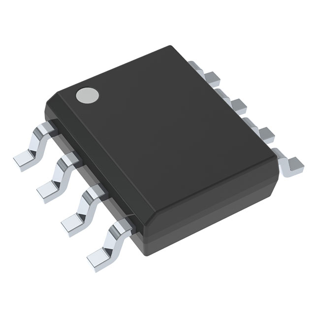
The TLC4502IDR from Texas Instruments is a high-performance, dual-channel CMOS operational amplifier designed for precision analog applications. Packaged in an 8-SOIC surface-mount configuration and supplied in Tape & Reel (TR), this IC is optimized for low-power, high-accuracy systems. With a 4.7 MHz gain bandwidth product (GBW) and an ultra-low input bias current of 1 pA, it ensures minimal signal distortion and high input impedance, making it ideal for sensor interfaces and data acquisition systems. The device operates over a 4 V to 6 V supply range, delivering 2.5 mA per channel while maintaining 10 µV input offset voltage for precision performance.
TLC4502IDR Features
- CMOS Technology: Ensures low power consumption and high input impedance.
- Dual-Channel Design: Two independent op-amps in a single package, saving board space.
- Low Input Bias Current (1 pA): Reduces errors in high-impedance circuits.
- High Slew Rate (2.5V/µs): Suitable for fast signal processing.
- Wide Supply Range (4 V–6 V): Flexible for battery-powered and industrial applications.
- 50 mA Output Current: Capable of driving moderate loads directly.
- ROHS3 Compliant & REACH Unaffected: Meets environmental and regulatory standards.
TLC4502IDR Applications
- Sensor Signal Conditioning: Ideal for amplifying low-level signals from thermocouples, strain gauges, and photodiodes.
- Active Filters: High GBW and low noise make it suitable for audio and communication filters.
- Portable & Battery-Powered Devices: Low current consumption extends battery life in handheld instruments.
- Data Acquisition Systems: Precision offset and low bias current ensure accurate analog-to-digital conversion.
- Medical Instrumentation: Reliable performance in ECG amplifiers and patient monitoring systems.
Conclusion of TLC4502IDR
The TLC4502IDR stands out for its ultra-low input bias current, precision offset voltage, and dual-channel integration, making it a versatile choice for high-impedance, low-power, and precision analog designs. Its CMOS architecture and robust performance metrics position it as a superior alternative to traditional bipolar op-amps in applications demanding accuracy and efficiency. Engineers can leverage its benefits in sensor interfaces, portable electronics, and signal processing systems where reliability and power efficiency are critical.
Tech Specifications
TLC4502IDR Documents
Download datasheets and manufacturer documentation for TLC4502IDR
 TLC4501/A, TLC4502/A
  Design 25/Feb/2022
 Shopping Guide


.png?x-oss-process=image/format,webp/resize,h_32)


