
Texas Instruments
TLE2062ACD
OP Amps, Buffer Amps ICs


.png?x-oss-process=image/format,webp/resize,p_30)


TLE2062ACD Description
TLE2062ACD Description
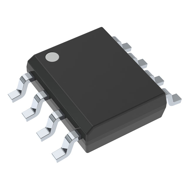
The TLE2062ACD from Texas Instruments is a dual-channel, high-performance JFET-input operational amplifier housed in an 8-SOIC package. Designed for precision applications, it operates over a wide supply voltage range of 7V to 36V, making it suitable for both industrial and automotive systems. With an ultra-low input bias current of 4 pA and a gain bandwidth product of 2 MHz, it excels in high-impedance signal conditioning and filtering. The device features low supply current (625µA per channel) and high output current drive (80 mA per channel), ensuring efficient power management and robust performance in demanding environments.
TLE2062ACD Features
- Low Input Bias Current (4 pA): Ideal for high-impedance sensor interfaces and medical instrumentation.
- Wide Supply Range (7V–36V): Supports flexible power configurations in industrial and automotive designs.
- High Slew Rate (3.4V/µs): Enables fast signal response in data acquisition and control systems.
- Low Offset Voltage (800 µV): Enhances accuracy in precision amplification and measurement circuits.
- RoHS3 Compliant & REACH Unaffected: Meets environmental and regulatory standards for global deployment.
- JFET Input Stage: Provides high input impedance and minimal noise, critical for audio and instrumentation.
TLE2062ACD Applications
- Sensor Signal Conditioning: Amplifies low-level signals from thermocouples, strain gauges, and photodiodes.
- Active Filters & Preamplifiers: Leverages low noise and high bandwidth for audio and communication systems.
- Test & Measurement Equipment: Ensures precision in oscilloscopes, multimeters, and data loggers.
- Industrial Control Systems: Operates reliably in PLCs, motor drives, and process control loops.
- Battery-Powered Devices: Optimizes efficiency in portable medical devices and handheld instruments.
Conclusion of TLE2062ACD
The TLE2062ACD stands out for its low power consumption, high precision, and robust supply voltage tolerance, making it a versatile choice for engineers designing high-performance analog circuits. While marked as Last Time Buy, its JFET architecture and superior specifications ensure it remains a preferred solution for legacy and new designs requiring low-noise, high-impedance amplification. Ideal for industrial, automotive, and instrumentation applications, it balances performance with reliability in critical systems.
Tech Specifications
TLE2062ACD Documents
Download datasheets and manufacturer documentation for TLE2062ACD
 TLE206x/A/B
  EOL 22/May/2023
  TLE206x/A/B
  Mult Devices Font 21/Apr/2018 Design 25/Feb/2022
 Shopping Guide


.png?x-oss-process=image/format,webp/resize,h_32)


