
Texas Instruments
TLE2082AID
OP Amps, Buffer Amps ICs


.png?x-oss-process=image/format,webp/resize,p_30)


TLE2082AID Description
TLE2082AID Description
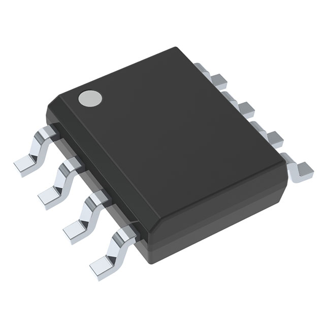
The TLE2082AID is a high-performance, dual-channel operational amplifier (op-amp) from Texas Instruments, designed for a wide range of applications where precision and reliability are paramount. This op-amp features a JFET input stage, providing high input impedance and low input bias current, making it ideal for sensitive signal processing tasks. The TLE2082AID operates from a wide supply voltage range of 4.5 V to 38 V, ensuring compatibility with various power supply configurations. With a gain bandwidth product of 10 MHz and a slew rate of 40 V/µs, the TLE2082AID delivers exceptional performance in both speed and accuracy. The device is housed in an 8SOIC package, suitable for surface-mount applications, and is available in a tube package format.
TLE2082AID Features
- Wide Supply Voltage Range: The TLE2082AID can operate from a supply voltage as low as 4.5 V up to 38 V, making it versatile for different power supply requirements.
- High Input Impedance: The JFET input stage ensures high input impedance and low input bias current (20 pA), which is crucial for applications requiring minimal loading effects on the signal source.
- High Gain Bandwidth Product: With a gain bandwidth product of 10 MHz, the TLE2082AID can handle high-frequency signals with minimal distortion, ensuring precise amplification.
- Fast Slew Rate: The 40 V/µs slew rate allows the op-amp to respond quickly to changes in input signals, making it suitable for applications requiring fast transient response.
- Low Input Offset Voltage: The input offset voltage of 700 µV ensures high accuracy in signal processing, minimizing errors in the output signal.
- Dual Channel Design: The TLE2082AID features two independent op-amp channels, each capable of sourcing up to 48 mA of output current, providing flexibility in circuit design.
- Surface Mount Compatibility: The 8SOIC package format is ideal for surface-mount technology (SMT), enabling compact and reliable designs.
- Compliance and Reliability: The TLE2082AID is REACH unaffected and RoHS3 compliant, ensuring environmental and safety standards are met. It also has a moisture sensitivity level (MSL) of 1, indicating unlimited shelf life under standard conditions.
TLE2082AID Applications
The TLE2082AID is well-suited for a variety of applications where precision, speed, and reliability are critical. Some specific use cases include:
- Precision Signal Amplification: Ideal for amplifying low-level signals in instrumentation and measurement systems, ensuring high accuracy and minimal signal degradation.
- High-Speed Signal Processing: Suitable for applications requiring fast transient response, such as in high-speed analog-to-digital converters (ADCs) and digital-to-analog converters (DACs).
- Medical Equipment: The low input bias current and high input impedance make the TLE2082AID suitable for medical devices where minimal loading on the signal source is essential.
- Automotive Electronics: The wide supply voltage range and robust performance make it suitable for automotive applications where power supply voltages can vary significantly.
- Industrial Control Systems: The TLE2082AID can be used in industrial control systems for signal conditioning and amplification, ensuring reliable operation in harsh environments.
Conclusion of TLE2082AID
The TLE2082AID from Texas Instruments is a versatile and high-performance dual-channel op-amp that offers a combination of precision, speed, and reliability. Its wide supply voltage range, high input impedance, and fast slew rate make it suitable for a wide range of applications, from precision signal amplification to high-speed signal processing. The device's compliance with environmental and safety standards, along with its surface-mount compatibility, ensures that it meets the demands of modern electronics design. Whether used in medical equipment, automotive electronics, or industrial control systems, the TLE2082AID provides the performance and reliability needed to ensure accurate and efficient signal processing.
Tech Specifications
TLE2082AID Documents
Download datasheets and manufacturer documentation for TLE2082AID
 Product Discontinuance Notification (PDF)
  Mechanical Outline Drawing
  Qualification of Alternate Material Set for Assembly with Au Wire and Cu as Additional Wire Base Metal Option for Select SOIC Package Devices (PDF)
  TLE2082AID Symbol & Footprint by SnapMagic
  TLE2081 TLE2082 TLE2084 EMI Immunity Performance
  TLE2082, TLE2082A PSpice Model
 Shopping Guide


.png?x-oss-process=image/format,webp/resize,h_32)


