
Texas Instruments
TLV172IDCKT
OP Amps, Buffer Amps ICs


.png?x-oss-process=image/format,webp/resize,p_30)


TLV172IDCKT Description
TLV172IDCKT Description
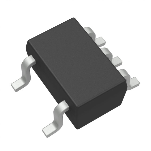
The TLV172IDCKT is a general-purpose operational amplifier (op-amp) from Texas Instruments, designed for a wide range of applications requiring high performance and reliability. This op-amp is housed in a SC70-5 package, making it suitable for surface-mount applications. It features a broad supply voltage range, from a minimum of 4.5 V to a maximum of 36 V, allowing it to operate efficiently across various power supply configurations. The TLV172IDCKT boasts a gain bandwidth product of 10 MHz, ensuring high-frequency performance and stability. Its slew rate of 10 V/µs further enhances its ability to handle fast signal transitions without distortion.
TLV172IDCKT Features
- Wide Supply Voltage Range: The TLV172IDCKT operates from 4.5 V to 36 V, providing flexibility in power supply design.
- High Gain Bandwidth Product: With a gain bandwidth product of 10 MHz, this op-amp delivers high performance in signal processing applications.
- Low Input Bias Current: The input bias current is as low as 10 pA, minimizing the impact on sensitive input signals.
- Low Input Offset Voltage: The voltage input offset is only 500 µV, ensuring accurate signal amplification.
- High Output Current: Each channel can deliver up to 75 mA, making it suitable for driving various loads.
- Low Supply Current: The device consumes only 1.6 mA, contributing to energy efficiency in power-sensitive designs.
- Compliance and Reliability: The TLV172IDCKT is REACH unaffected and RoHS3 compliant, ensuring environmental safety and regulatory compliance. It also has a moisture sensitivity level (MSL) of 1, making it suitable for unlimited storage conditions.
- Packaging: Available in a tape & reel (TR) package, it is ideal for automated assembly processes.
TLV172IDCKT Applications
The TLV172IDCKT is well-suited for a variety of applications due to its versatile performance characteristics. Some key applications include:
- Signal Conditioning: Ideal for amplifying and conditioning low-level signals in sensor interfaces and data acquisition systems.
- Audio Amplification: Its low input bias current and high output current make it suitable for driving audio signals in consumer electronics.
- Power Management: The wide supply voltage range and low supply current make it a good fit for power management circuits in portable devices.
- Industrial Control Systems: The high slew rate and gain bandwidth product enable it to handle fast signal transitions in industrial automation and control systems.
- Medical Equipment: The low input offset voltage and high accuracy make it suitable for medical devices requiring precise signal processing.
Conclusion of TLV172IDCKT
The TLV172IDCKT from Texas Instruments stands out as a versatile and high-performance general-purpose operational amplifier. Its wide supply voltage range, high gain bandwidth product, and low input bias current make it suitable for a broad range of applications. The device's compliance with environmental and regulatory standards, along with its low supply current and high output current, further enhance its appeal. Whether used in signal conditioning, audio amplification, power management, industrial control systems, or medical equipment, the TLV172IDCKT offers reliable performance and efficiency.
Tech Specifications
TLV172IDCKT Documents
Download datasheets and manufacturer documentation for TLV172IDCKT
 Mechanical Outline Drawing
  TLV172IDCKT Symbol & Footprint by SnapMagic
  Full-wave rectifier circuit (Rev. A)
  TLVx172 TINA-TI Reference Design (Rev. A)
  TLVX172 TINA-TI Spice Model (Rev. A) TLVX172 PSpice Model (Rev. A)
 Shopping Guide


.png?x-oss-process=image/format,webp/resize,h_32)


