
Texas Instruments
TLV2711CDBVRG4
OP Amps, Buffer Amps ICs


.png?x-oss-process=image/format,webp/resize,p_30)


TLV2711CDBVRG4 Description
TLV2711CDBVRG4 Description
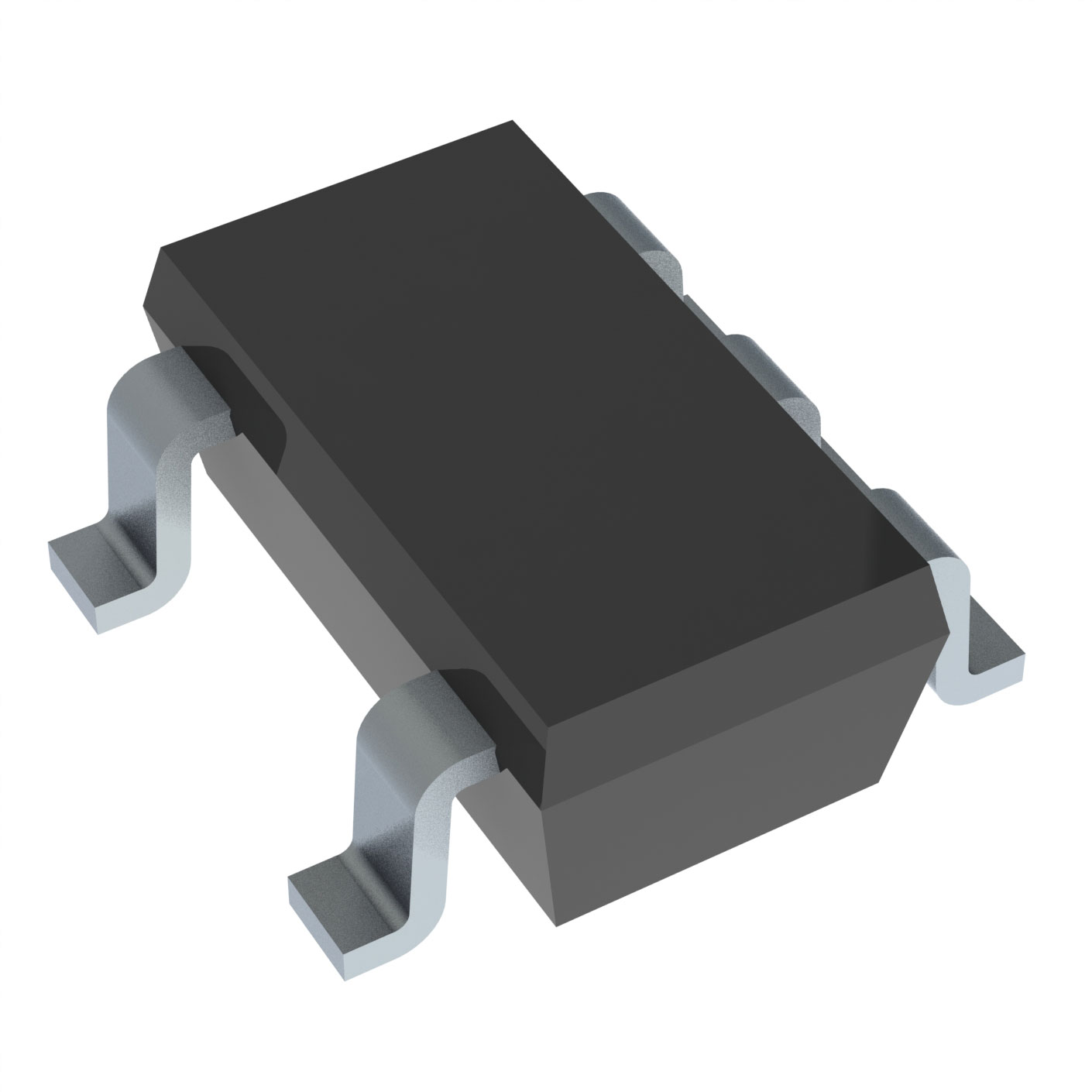
The TLV2711CDBVRG4 is a general-purpose operational amplifier from Texas Instruments, designed for a wide range of applications requiring high performance and low power consumption. This op-amp is part of the LinCMOS™ series and is housed in a compact SOT23-5 package, making it ideal for surface-mount applications. It operates over a supply voltage range of 2.7 V to 10 V, ensuring flexibility in various power supply configurations. The TLV2711CDBVRG4 is REACH unaffected and RoHS3 compliant, adhering to stringent environmental and safety standards.
TLV2711CDBVRG4 Features
- Wide Supply Voltage Range: The TLV2711CDBVRG4 operates from a minimum supply voltage of 2.7 V up to a maximum of 10 V, providing versatility in different circuit designs.
- Low Input Bias Current: With an input bias current of just 1 pA, this op-amp minimizes the loading effect on high-impedance sources, ensuring accurate signal processing.
- Low Power Consumption: Consuming only 13 µA of supply current, the TLV2711CDBVRG4 is highly efficient, making it suitable for battery-powered and low-power applications.
- High Gain Bandwidth Product: A gain bandwidth product of 65 kHz ensures high-frequency performance, making it ideal for applications requiring wide bandwidth.
- Low Input Offset Voltage: The 450 µV input offset voltage ensures high accuracy and precision in signal amplification.
- High Output Current: Capable of delivering up to 50 mA per channel, the TLV2711CDBVRG4 can drive heavy loads without significant voltage drop.
- Moisture Sensitivity Level: With an MSL of 1 (Unlimited), the TLV2711CDBVRG4 is suitable for use in environments with varying humidity levels, without the need for special handling.
- Operating Temperature Range: The TLV2711CDBVRG4 operates reliably within a temperature range of 0°C to 70°C, making it suitable for a wide range of industrial and consumer applications.
TLV2711CDBVRG4 Applications
The TLV2711CDBVRG4 is well-suited for a variety of applications due to its combination of low power consumption, high performance, and compact size. Specific use cases include:
- Signal Conditioning: Ideal for amplifying and conditioning low-level signals in sensor interfaces, ensuring high accuracy and precision.
- Battery-Powered Devices: Its low power consumption makes it suitable for portable and battery-powered applications, such as handheld devices and wearable technology.
- Consumer Electronics: The compact SOT23-5 package and wide supply voltage range make it a perfect fit for consumer electronics, where space and power efficiency are critical.
- Industrial Control Systems: The high output current and wide operating temperature range make it suitable for industrial control systems that require reliable and robust performance.
- Medical Devices: The low input bias current and high accuracy make it suitable for medical devices where signal integrity is paramount.
Conclusion of TLV2711CDBVRG4
The TLV2711CDBVRG4 from Texas Instruments is a versatile and high-performance operational amplifier that offers significant advantages over similar models. Its wide supply voltage range, low power consumption, and high output current make it suitable for a wide range of applications, from consumer electronics to industrial control systems. The compact SOT23-5 package ensures ease of integration in space-constrained designs, while its low input bias current and high gain bandwidth product ensure high accuracy and precision. The TLV2711CDBVRG4 is an excellent choice for designers looking for a reliable, efficient, and high-performance op-amp solution.
Tech Specifications
TLV2711CDBVRG4 Documents
Download datasheets and manufacturer documentation for TLV2711CDBVRG4
 TLV2711, TLV2711Y
  TLV2711, TLV2711Y
 Shopping Guide


.png?x-oss-process=image/format,webp/resize,h_32)


