
Texas Instruments
TLV2721CDBVT
OP Amps, Buffer Amps ICs


.png?x-oss-process=image/format,webp/resize,p_30)


TLV2721CDBVT Description
TLV2721CDBVT Description
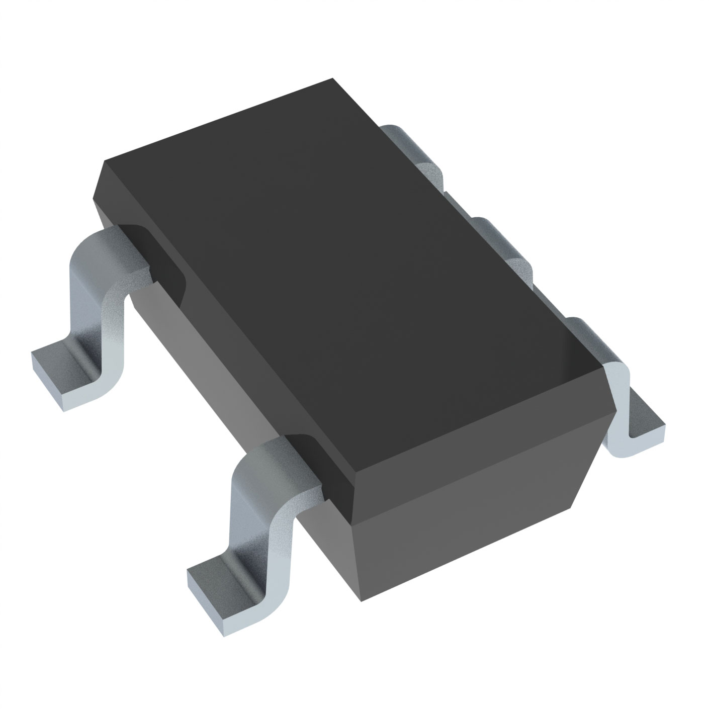
The TLV2721CDBVT is a general-purpose operational amplifier (op-amp) from Texas Instruments, designed for a wide range of applications requiring high performance in a compact package. This op-amp is part of the LinCMOS™ series and is housed in a surface-mount SOT23-5 package, making it suitable for space-constrained designs. The TLV2721CDBVT operates over a supply voltage range of 2.7 V to 10 V, providing flexibility in power supply options. It features a gain bandwidth product of 510 kHz, a slew rate of 0.25 V/µs, and a supply current of just 110 µA, making it an energy-efficient choice for battery-powered and low-power applications.
TLV2721CDBVT Features
- Wide Supply Voltage Range: The TLV2721CDBVT operates from a minimum supply voltage of 2.7 V up to a maximum of 10 V, offering versatility in power supply requirements.
- Low Input Bias Current: With an input bias current of only 1 pA, the TLV2721CDBVT minimizes the impact of bias currents on signal integrity, making it ideal for high-impedance applications.
- Low Offset Voltage: A voltage input offset of 500 µV ensures accurate signal processing and minimal error in precision applications.
- High Output Current: The op-amp can deliver up to 50 mA per channel, enabling it to drive moderate loads directly without additional buffering.
- Energy Efficiency: The low supply current of 110 µA makes the TLV2721CDBVT suitable for low-power applications, such as portable devices and battery-operated systems.
- Compliance and Reliability: The TLV2721CDBVT is ROHS3 compliant and REACH unaffected, ensuring it meets environmental and regulatory standards. It also has a moisture sensitivity level (MSL) of 1, making it suitable for extended storage and handling.
- Operating Temperature Range: The device operates reliably within a temperature range of 0°C to 70°C, making it suitable for a variety of industrial and consumer applications.
TLV2721CDBVT Applications
The TLV2721CDBVT is well-suited for a variety of applications due to its combination of performance and low power consumption. Some specific use cases include:
- Signal Conditioning: Ideal for amplifying and conditioning signals in sensor interfaces, where low input bias current and low offset voltage are critical for maintaining signal accuracy.
- Battery-Powered Devices: Its low supply current and wide operating voltage range make it a perfect fit for portable electronics and IoT devices that require long battery life.
- Consumer Electronics: Suitable for applications such as audio amplifiers, where the op-amp's performance characteristics ensure high-fidelity signal processing.
- Industrial Control Systems: The op-amp's robustness and compliance with environmental standards make it suitable for use in industrial control systems and automation equipment.
Conclusion of TLV2721CDBVT
The TLV2721CDBVT from Texas Instruments is a versatile and high-performance general-purpose op-amp that offers a balance of low power consumption, wide supply voltage range, and excellent signal processing capabilities. Its low input bias current and low offset voltage make it particularly suitable for high-impedance and precision applications. The compact SOT23-5 package and surface-mount design allow for easy integration into space-constrained designs. The TLV2721CDBVT is an excellent choice for engineers looking to optimize their designs for performance, power efficiency, and reliability.
Tech Specifications
TLV2721CDBVT Documents
Download datasheets and manufacturer documentation for TLV2721CDBVT
 Additional Assembly sites 21/Sep/2021
  TLV2721, TLV2721Y
  EOL 22/May/2023
  TLV2721, TLV2721Y
 Shopping Guide


.png?x-oss-process=image/format,webp/resize,h_32)


