

Texas Instruments
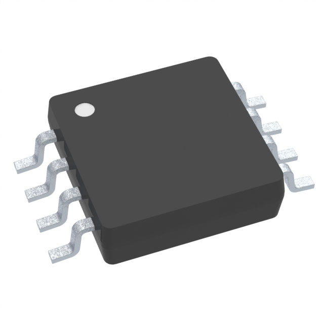
TLV272IDGK
OP Amps, Buffer Amps ICs

Not available to buy online? Want the lower wholesale price? Please Send RFQ to get best price, we will respond immediately


.png?x-oss-process=image/format,webp/resize,p_30)


TLV272IDGK Description
TLV272IDGK Description
The TLV272IDGK from Texas Instruments is a high-performance, general-purpose operational amplifier (op-amp) designed for precision analog applications. Packaged in an 8-VSSOP form factor, this dual-channel op-amp operates over a wide supply voltage range of 2.7V to 16V, making it versatile for both low-voltage and industrial applications. With a 3 MHz gain bandwidth product (GBW) and a slew rate of 2.6V/µs, it delivers excellent signal fidelity and transient response. The device features an ultra-low input bias current of 1 pA and a low input offset voltage of 500 µV, ensuring high accuracy in sensitive circuits. Its ROHS3 compliance and REACH unaffected status make it environmentally friendly and suitable for global markets.
TLV272IDGK Features
- Low Power Consumption: Only 550µA per channel supply current, ideal for battery-powered systems.
- Wide Supply Range: Operates from 2.7V to 16V, accommodating diverse power environments.
- High Precision: 1 pA input bias current and 500 µV offset voltage for accurate signal conditioning.
- Fast Response: 3 MHz GBW and 2.6V/µs slew rate ensure robust performance in dynamic applications.
- Robust Packaging: 8-VSSOP surface-mount package with MSL 1 (Unlimited) rating for easy handling and assembly.
- Dual-Channel Design: Two independent op-amps in a compact footprint, saving board space.
TLV272IDGK Applications
The TLV272IDGK excels in precision and low-power applications, including:
- Sensor Signal Conditioning: Ideal for amplifying low-level signals from thermocouples, strain gauges, or photodiodes.
- Portable and Battery-Powered Devices: Due to its low quiescent current, it’s perfect for wearables, IoT sensors, and medical devices.
- Active Filters and Data Acquisition: The high GBW and slew rate make it suitable for anti-aliasing filters and ADC drivers.
- Industrial Control Systems: Operates reliably in harsh environments with wide voltage fluctuations.
Conclusion of TLV272IDGK
The TLV272IDGK combines precision, low power consumption, and robust performance, making it a standout choice for engineers designing analog circuits. Its wide supply range, low input bias current, and high-speed response cater to demanding applications in industrial, medical, and consumer electronics. With Texas Instruments' reputation for reliability, this op-amp is a dependable solution for enhancing signal integrity and system efficiency.
Tech Specifications
TLV272IDGK Documents
Download datasheets and manufacturer documentation for TLV272IDGK
Fab Site 29/Jun/2022 TLV271, TLV272, TLV274 TLV271, TLV272, TLV274 SOT23, VSSOP Cu Wire 28/Jun/2013 Copper Wire Revision C 24/Sep/2014 Related Parts


Shopping Guide


.png?x-oss-process=image/format,webp/resize,h_32)


©2025 ERSA Electronics Corporation.