
Texas Instruments
TLV2771CDBVT
OP Amps, Buffer Amps ICs


.png?x-oss-process=image/format,webp/resize,p_30)


TLV2771CDBVT Description
TLV2771CDBVT Description
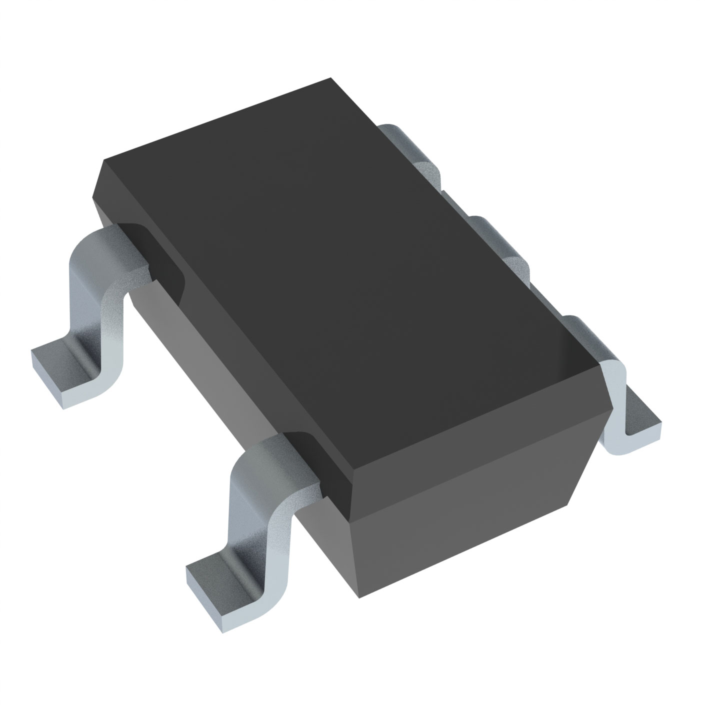
The TLV2771CDBVT is a high-performance, general-purpose operational amplifier (op-amp) designed for a wide range of applications. Manufactured by Texas Instruments, this op-amp is part of the Linear IC Chips category and is housed in a compact SOT23-5 package, making it ideal for surface-mount applications. The TLV2771CDBVT offers a broad supply voltage range, from a minimum of 2.5 V to a maximum of 5.5 V, ensuring compatibility with various power supply configurations. Its gain bandwidth product of 5.1 MHz and a slew rate of 10.5 V/µs provide excellent performance for high-frequency applications. The op-amp features a low input bias current of 2 pA and an input offset voltage of 500 µV, ensuring high precision in signal processing. With a supply current of just 1 mA and an output current per channel of 50 mA, the TLV2771CDBVT is both power-efficient and capable of driving significant loads.
TLV2771CDBVT Features
- Wide Supply Voltage Range: Operates from 2.5 V to 5.5 V, providing flexibility in power supply requirements.
- High Gain Bandwidth Product: 5.1 MHz ensures high-frequency performance, making it suitable for applications requiring fast signal processing.
- Low Input Bias Current: 2 pA minimizes the impact on sensitive input signals, ensuring high-precision measurements.
- Low Input Offset Voltage: 500 µV ensures accurate signal amplification and reduces errors in low-level signal processing.
- High Slew Rate: 10.5 V/µs allows for rapid response to input signal changes, ideal for high-speed applications.
- Power Efficiency: 1 mA supply current ensures minimal power consumption, making it suitable for battery-powered and low-power applications.
- High Output Current: 50 mA per channel allows the op-amp to drive significant loads, enhancing its versatility.
- Compact Packaging: SOT23-5 package is ideal for surface-mount applications, saving space on the PCB.
- Compliance and Reliability: REACH Unaffected and ROHS3 Compliant, ensuring environmental and regulatory standards are met. Moisture Sensitivity Level (MSL) of 1 (Unlimited) ensures reliability in various environmental conditions.
TLV2771CDBVT Applications
The TLV2771CDBVT is well-suited for a variety of applications due to its high performance and versatility. Some specific use cases include:
- Signal Conditioning: Ideal for amplifying and conditioning low-level signals in sensor applications, ensuring accurate and reliable measurements.
- Audio Processing: Its high gain bandwidth product and low input offset voltage make it suitable for audio signal processing, providing clear and distortion-free audio output.
- Industrial Control Systems: The op-amp's ability to drive significant loads and its wide supply voltage range make it ideal for industrial control systems, where robustness and reliability are critical.
- Consumer Electronics: The compact SOT23-5 package and power efficiency make it suitable for consumer electronics, where space and power consumption are key considerations.
- Medical Devices: High precision and low input bias current ensure accurate signal processing in medical devices, such as ECG and EEG machines.
Conclusion of TLV2771CDBVT
The TLV2771CDBVT is a versatile and high-performance general-purpose op-amp that offers a wide range of technical specifications and benefits. Its wide supply voltage range, high gain bandwidth product, low input bias current, and low input offset voltage make it suitable for a variety of applications, from signal conditioning to audio processing. The compact SOT23-5 package and power efficiency further enhance its appeal for space-constrained and low-power applications. With its compliance to environmental and regulatory standards, the TLV2771CDBVT is a reliable choice for engineers and designers looking for a robust and efficient op-amp solution.
Tech Specifications
TLV2771CDBVT Documents
Download datasheets and manufacturer documentation for TLV2771CDBVT
 Additional Assembly sites 21/Sep/2021
  TLV277x(A)
  EOL 22/May/2023
  TLV277x(A)
 Shopping Guide


.png?x-oss-process=image/format,webp/resize,h_32)


