
Texas Instruments
TLV2781CDBVT
OP Amps, Buffer Amps ICs


.png?x-oss-process=image/format,webp/resize,p_30)


TLV2781CDBVT Description
TLV2781CDBVT Description
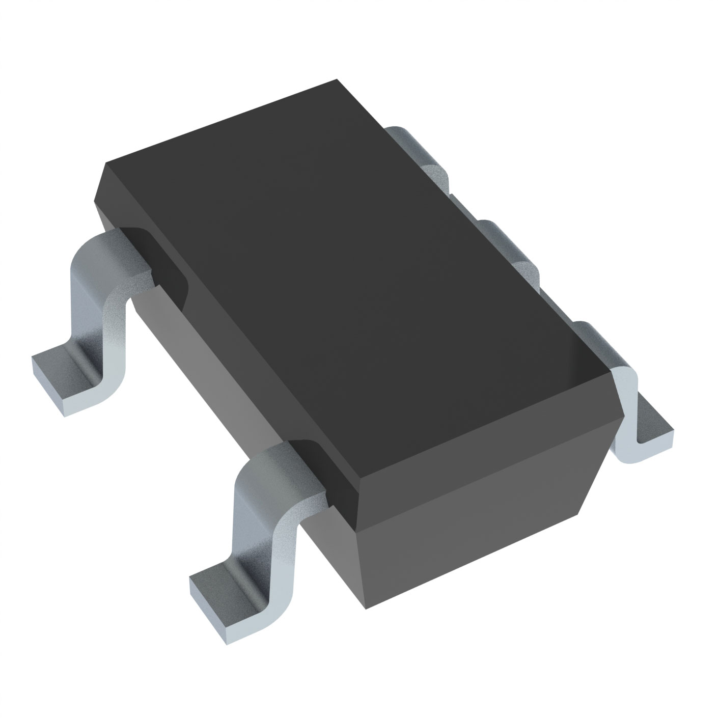
The TLV2781CDBVT is a general-purpose operational amplifier (op-amp) from Texas Instruments, designed for a wide range of applications requiring high performance and reliability. This op-amp is housed in a SOT23-5 package, making it suitable for surface-mount applications. It operates within a supply voltage range of 1.8 V to 3.6 V, providing flexibility for various power supply configurations. The TLV2781CDBVT features a gain bandwidth product of 8 MHz, ensuring high-frequency performance and stability. Its slew rate of 5 V/µs allows for fast transient response, making it ideal for applications requiring rapid signal processing. The op-amp also boasts a low input bias current of 2.5 pA and an input offset voltage of 250 µV, contributing to its high precision and accuracy. With a supply current of 650 µA and a maximum output current per channel of 23 mA, the TLV2781CDBVT offers efficient power usage and robust output capabilities. It is compliant with REACH and ROHS3 standards, ensuring environmental sustainability and regulatory adherence. The device operates within a temperature range of 0°C to 70°C, making it suitable for a variety of industrial and consumer applications. The TLV2781CDBVT is available in a tape and reel package, facilitating easy handling and integration into automated assembly processes.
TLV2781CDBVT Features
- Wide Supply Voltage Range: Operates from 1.8 V to 3.6 V, providing flexibility for various power supply configurations.
- High Gain Bandwidth Product: 8 MHz ensures high-frequency performance and stability.
- Fast Slew Rate: 5 V/µs allows for rapid transient response, making it suitable for high-speed signal processing.
- Low Input Bias Current: 2.5 pA ensures high precision and accuracy in signal processing.
- Low Input Offset Voltage: 250 µV contributes to high accuracy and reliability.
- Efficient Power Usage: Supply current of 650 µA ensures efficient power consumption.
- Robust Output Capability: Maximum output current per channel of 23 mA provides strong drive capabilities.
- Compliance and Sustainability: REACH Unaffected and ROHS3 Compliant, ensuring environmental sustainability and regulatory adherence.
- Wide Operating Temperature Range: 0°C to 70°C, suitable for a variety of industrial and consumer applications.
- Surface-Mount Packaging: SOT23-5 package is ideal for compact and automated assembly processes.
TLV2781CDBVT Applications
The TLV2781CDBVT is well-suited for a variety of applications due to its high performance and flexibility. Some specific use cases include:
- Consumer Electronics: Ideal for portable devices and battery-powered applications due to its wide supply voltage range and low power consumption.
- Industrial Control Systems: Its high precision and robust output capabilities make it suitable for precision control and signal conditioning in industrial environments.
- Medical Equipment: The low input bias current and low input offset voltage ensure high accuracy and reliability, making it suitable for medical devices requiring precise measurements.
- Automotive Electronics: The wide operating temperature range and robust performance make it suitable for automotive applications where reliability and precision are critical.
- Signal Processing: The high gain bandwidth product and fast slew rate make it ideal for applications requiring high-speed signal processing and amplification.
Conclusion of TLV2781CDBVT
The TLV2781CDBVT from Texas Instruments is a versatile and high-performance operational amplifier designed for a wide range of applications. Its wide supply voltage range, high gain bandwidth product, and fast slew rate make it suitable for high-speed and high-precision signal processing. The low input bias current and low input offset voltage ensure high accuracy and reliability, while its efficient power usage and robust output capabilities make it ideal for a variety of industrial and consumer applications. Compliance with REACH and ROHS3 standards ensures environmental sustainability and regulatory adherence. The TLV2781CDBVT is an excellent choice for designers seeking a reliable and high-performance op-amp for their next project.
Tech Specifications
TLV2781CDBVT Documents
Download datasheets and manufacturer documentation for TLV2781CDBVT
 Additional Assembly sites 21/Sep/2021
  TLV2780-85, TLV278xA
  TLV2780-85, TLV278xA
 Shopping Guide


.png?x-oss-process=image/format,webp/resize,h_32)


