
Texas Instruments
TLV27L2CDGKR
OP Amps, Buffer Amps ICs


.png?x-oss-process=image/format,webp/resize,p_30)


TLV27L2CDGKR Description
TLV27L2CDGKR Description
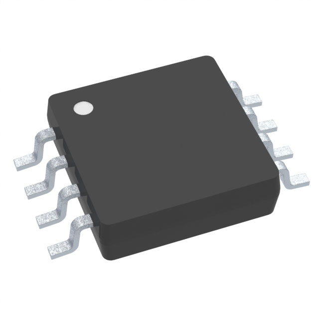
The TLV27L2CDGKR is a high-performance, general-purpose operational amplifier (op-amp) from Texas Instruments, designed to meet the demanding requirements of modern electronic systems. This dual-channel op-amp is housed in an 8-pin VSSOP package, making it suitable for surface-mount applications. It offers a wide supply voltage range from 2.7 V to 16 V, ensuring compatibility with a variety of power supply configurations. The TLV27L2CDGKR is optimized for low power consumption, with a supply current of just 7 µA per channel, making it ideal for battery-powered and energy-efficient designs.
TLV27L2CDGKR Features
- Wide Supply Voltage Range: The TLV27L2CDGKR operates from a supply voltage range of 2.7 V to 16 V, providing flexibility in power supply design.
- Low Power Consumption: With a supply current of only 7 µA per channel, this op-amp is highly efficient, making it suitable for low-power applications.
- High Gain Bandwidth Product: The gain bandwidth product of 160 kHz ensures high-frequency performance, suitable for a wide range of signal processing tasks.
- Low Input Bias Current: The input bias current is as low as 1 pA, minimizing the impact on sensitive input signals.
- Low Input Offset Voltage: An input offset voltage of 500 µV ensures high accuracy and stability in signal amplification.
- High Slew Rate: The slew rate of 0.06 V/µs allows for fast response times, making it suitable for applications requiring rapid signal changes.
- Dual Channel Design: The TLV27L2CDGKR features two independent op-amp channels, providing flexibility in circuit design and the ability to handle multiple signals simultaneously.
- Compliance and Reliability: The device is REACH unaffected and RoHS3 compliant, ensuring environmental and regulatory standards are met. It also has a moisture sensitivity level (MSL) of 1 (unlimited), making it suitable for various manufacturing environments.
TLV27L2CDGKR Applications
The TLV27L2CDGKR is well-suited for a variety of applications due to its versatile performance characteristics. Some specific use cases include:
- Signal Conditioning: Ideal for amplifying and conditioning low-level signals in sensors and transducers.
- Analog Signal Processing: Suitable for applications requiring high-frequency signal processing, such as audio and communication systems.
- Battery-Powered Devices: The low power consumption makes it perfect for portable and battery-operated equipment.
- Industrial Control Systems: The wide supply voltage range and high performance make it suitable for industrial applications where reliability and accuracy are critical.
- Medical Equipment: The low input bias current and offset voltage ensure high accuracy, making it suitable for medical devices that require precise signal processing.
Conclusion of TLV27L2CDGKR
The TLV27L2CDGKR from Texas Instruments is a versatile and high-performance general-purpose operational amplifier that offers a combination of low power consumption, wide supply voltage range, and high performance. Its dual-channel design, low input bias current, and low input offset voltage make it an excellent choice for a wide range of applications, from signal conditioning to industrial control systems. The device's compliance with environmental and regulatory standards further enhances its suitability for modern electronic designs. Whether in portable devices, medical equipment, or industrial applications, the TLV27L2CDGKR provides reliable and efficient performance, making it a standout choice in its category.
Tech Specifications
TLV27L2CDGKR Documents
Download datasheets and manufacturer documentation for TLV27L2CDGKR
 TLV27L1, TLV27L2 Datasheet
  8-VSSOP
  SOT23, VSSOP Cu Wire 28/Jun/2013 Copper Wire Revision C 24/Sep/2014
 Shopping Guide


.png?x-oss-process=image/format,webp/resize,h_32)


