
Texas Instruments
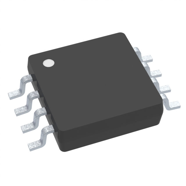
TLV3542IDGKR
OP Amps, Buffer Amps ICs


.png?x-oss-process=image/format,webp/resize,p_30)


TLV3542IDGKR Description
TLV3542IDGKR Description
The TLV3542IDGKR is a high-performance, dual-channel operational amplifier (op amp) designed and manufactured by Texas Instruments. This CMOS op amp is known for its excellent DC precision, high bandwidth, and low power consumption, making it ideal for a wide range of applications. With a supply voltage range of 2.5 V to 5.5 V, it can operate in various power supply environments. The device is RoHS3 compliant and REACH unaffected, ensuring environmental compliance for your designs.
TLV3542IDGKR Features
- Voltage - Supply Span (Max): 5.5 V
- Voltage - Supply Span (Min): 2.5 V
- Gain Bandwidth Product: 100 MHz
- -3db Bandwidth: 200 MHz
- Slew Rate: 150V/µs
- Current - Input Bias: 3 pA
- Current - Supply: 5.2mA (x2 Channels)
- Current - Output / Channel: 100 mA
- Voltage - Input Offset: 2 mV
- Mounting Type: Surface Mount
- Package: Tape & Reel (TR)
- Number of Circuits: 2
- Moisture Sensitivity Level (MSL): 2 (1 Year)
- ECCN: EAR99
- HTSUS: 8542.33.0001
- Product Status: Active
TLV3542IDGKR Applications
The TLV3542IDGKR is well-suited for applications that require high precision and performance, such as:
- Audio Applications: Due to its high slew rate and bandwidth, it is ideal for audio preamplifiers and line drivers.
- Data Acquisition Systems: The low input bias current and low voltage offset make it suitable for high-resolution data acquisition systems.
- Sensor Conditioning: Its low noise and high precision make it an excellent choice for conditioning signals from sensors in industrial and medical applications.
- Portable Devices: The low power consumption and wide supply voltage range make it suitable for battery-powered devices.
Conclusion of TLV3542IDGKR
The TLV3542IDGKR from Texas Instruments is a versatile, dual-channel op amp that offers a combination of high performance and low power consumption. Its wide supply voltage range, low input bias current, and high slew rate make it an excellent choice for a variety of applications, from audio to data acquisition. With its RoHS3 compliance and REACH unaffected status, it is also an environmentally friendly option for your designs. The TLV3542IDGKR's unique features and advantages make it a standout choice in the market for high-performance op amps.
Tech Specifications
TLV3542IDGKR Documents
Download datasheets and manufacturer documentation for TLV3542IDGKR
 Mechanical Outline Drawing
  Product Change Notification (PDF)
  TLV3542IDGKR Symbol & Footprint by SnapMagic
  TLV354x TINA-TI Reference Design TLV354x TINA-TI Reference Design (Rev. A)
  TLV354x PSpice Model TLV354x TINA-TI Spice Model (Rev. A) TLV354x PSpice Model (Rev. A) TLV354x TINA-TI Spice Model
 Shopping Guide


.png?x-oss-process=image/format,webp/resize,h_32)


