
Texas Instruments
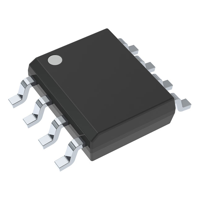
TLV4112ID
OP Amps, Buffer Amps ICs


.png?x-oss-process=image/format,webp/resize,p_30)


TLV4112ID Description
TLV4112ID Description
The TLV4112ID is a high-performance, general-purpose operational amplifier (op-amp) from Texas Instruments, designed for a wide range of applications requiring precision and reliability. This dual-channel op-amp features a supply voltage range of 2.5 V to 6 V, making it suitable for both low-power and standard voltage systems. With a gain bandwidth product of 2.7 MHz, the TLV4112ID ensures high-frequency performance while maintaining stability. The device offers a low input bias current of 0.3 pA, which is crucial for applications where high impedance sources are used. Additionally, the TLV4112ID boasts a low input offset voltage of 175 µV, ensuring accurate signal processing and minimal errors in precision circuits.
TLV4112ID Features
- Supply Voltage Range: The TLV4112ID operates within a supply voltage range of 2.5 V to 6 V, providing flexibility for various power supply configurations.
- Gain Bandwidth Product: With a gain bandwidth product of 2.7 MHz, this op-amp delivers high-frequency performance suitable for demanding applications.
- Low Input Bias Current: The low input bias current of 0.3 pA minimizes the loading effect on high impedance sources, ensuring accurate signal amplification.
- Low Input Offset Voltage: The low input offset voltage of 175 µV enhances the precision of the amplifier, making it ideal for applications requiring high accuracy.
- High Slew Rate: A slew rate of 1.57 V/µs allows the TLV4112ID to handle fast-changing signals without distortion.
- High Output Current: Each channel can provide up to 320 mA of output current, making it capable of driving heavy loads.
- Low Supply Current: The device consumes only 700 µA per channel, making it energy-efficient and suitable for battery-powered applications.
- Surface Mount Technology: The surface mount package ensures easy integration into compact designs and high-density PCB layouts.
- Compliance and Reliability: The TLV4112ID is REACH unaffected and RoHS3 compliant, ensuring environmental safety and regulatory compliance. It also has a moisture sensitivity level (MSL) of 1, making it suitable for a wide range of manufacturing environments.
TLV4112ID Applications
The TLV4112ID is ideal for a variety of applications due to its versatile performance characteristics. Some specific use cases include:
- Signal Conditioning: The low input bias current and low input offset voltage make it suitable for conditioning signals from high impedance sensors, such as those used in medical equipment and precision measurement instruments.
- Audio Amplification: The high slew rate and gain bandwidth product ensure high-fidelity audio performance, making it suitable for audio processing circuits.
- Industrial Control Systems: The device's ability to handle high output currents and its wide supply voltage range make it ideal for driving actuators and other industrial control applications.
- Consumer Electronics: The TLV4112ID's low power consumption and compact surface mount package make it suitable for portable devices and consumer electronics where space and power efficiency are critical.
Conclusion of TLV4112ID
The TLV4112ID from Texas Instruments is a versatile and high-performance general-purpose operational amplifier that offers a combination of precision, high-frequency performance, and low power consumption. Its low input bias current, low input offset voltage, and high slew rate make it suitable for a wide range of applications, from precision signal conditioning to high-fidelity audio amplification. The device's compliance with environmental and regulatory standards, along with its surface mount package, ensures ease of integration and reliability in various manufacturing environments. Whether used in medical equipment, industrial control systems, or consumer electronics, the TLV4112ID stands out as a reliable and efficient choice for engineers and designers.
Tech Specifications
TLV4112ID Documents
Download datasheets and manufacturer documentation for TLV4112ID
 Mechanical Outline Drawing
  Qualification of Alternate Material Set for Assembly with Au Wire and Cu as Additional Wire Base Metal Option for Select SOIC Package Devices (PDF)
  TLV4112ID Symbol & Footprint by SnapMagic
  TLV4110 TLV4111 TLV4112 TLV4113 EMI Immunity Performance TLV4110 TLV4111 TLV4112 TLV4113 EMI Immunity Performance (Rev. A)
  TLV4111 TINA-TI Reference Design (Rev. A) TLV4111 TINA-TI Reference Design
  TLV4111 PSpice Model TLV4111 PSpice Model (Rev. A) TLV4111 TINA-TI Spice Model TLV4111 TINA-TI Spice Model (Rev. A) TLV411xB PSpice 2.7V Supply Voltage Model TLV411xA PSpice 5V Supply Voltage Model
 Shopping Guide


.png?x-oss-process=image/format,webp/resize,h_32)


