
 German
 Japanese
 Portuguese
 Korea
Korea
 Mexico
 Dutch
Dutch


Texas Instruments
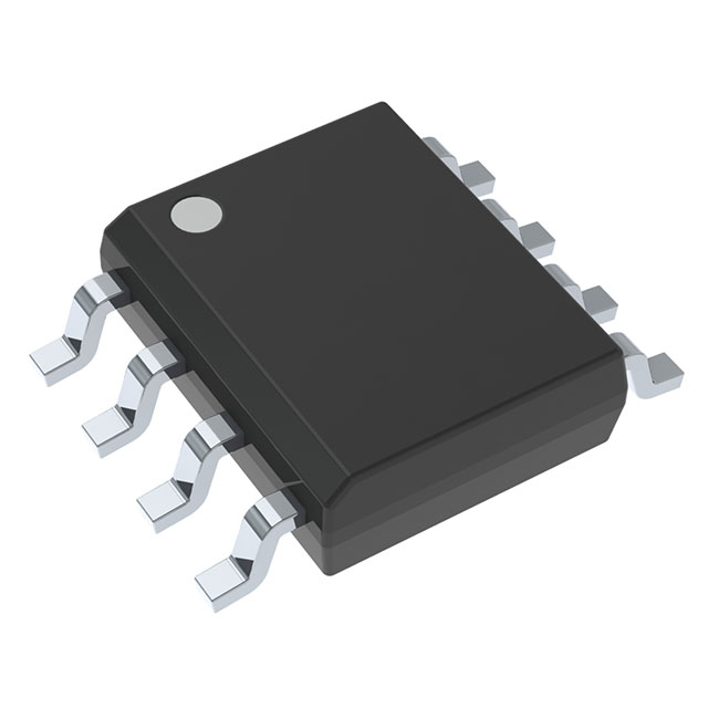
TLV9002QDRQ1

Why Choose Us?
Professional Platform
B2B & B2C purchasingDelivery at full speed
1-2 days deliveryWide variety
Original manufacturers365 days guarantee
Responsible quality
.png)


Tech Specifications
TLV9002QDRQ1 Description
The Texas Instruments TLV9002QDRQ1 is a high-performance, low-power, single-supply, monolithic operational amplifier (op-amp) designed for a wide range of applications.
Description:
The TLV9002QDRQ1 is a precision op-amp that offers low input offset voltage, low input bias current, and low noise performance. It is available in a small 8-pin QFN package, making it suitable for portable and space-constrained applications.
Features:
- Low Input Offset Voltage: The TLV9002QDRQ1 has an input offset voltage of typically 0.6 mV, which is ideal for precision applications.
- Low Input Bias Current: The input bias current is typically 1 pA, which makes it suitable for use with high-impedance inputs.
- Low Noise: The TLV9002QDRQ1 has a low noise level of 8 nV/√Hz, making it suitable for use in sensitive applications.
- Wide Supply Voltage Range: The op-amp can operate on a supply voltage range of 2.7 V to 10.8 V, making it suitable for a wide range of applications.
- High Output Drive Capability: The TLV9002QDRQ1 can drive capacitive loads up to 10 pF, making it suitable for driving high-capacity loads.
- Low Power Consumption: The op-amp consumes low power, typically 330 µA, which makes it suitable for battery-powered applications.
Applications:
The TLV9002QDRQ1 is suitable for a wide range of applications, including:
- Medical Instruments: The low input offset voltage and low noise make it ideal for use in medical instruments such as blood pressure monitors and pulse oximeters.
- Industrial Control Systems: The high output drive capability and wide supply voltage range make it suitable for use in industrial control systems.
- Audio Equipment: The low noise and low distortion characteristics make it suitable for use in audio equipment such as microphone preamps and headphone amplifiers.
- Battery-Powered Devices: The low power consumption makes it suitable for use in battery-powered devices such as portable audio recorders and hearing aids.
- Measurement and Test Equipment: The low input offset voltage and low drift make it suitable for use in measurement and test equipment such as oscilloscopes and signal generators.
In summary, the Texas Instruments TLV9002QDRQ1 is a high-performance, low-power, single-supply op-amp that offers excellent precision and noise performance, making it suitable for a wide range of applications.
FAQ
| Quantity | Unit Price | Ext. Price |
|---|---|---|
| 1+ | $0.38057 | $0.38 |
| 10+ | $0.37200 | $3.72 |
| 30+ | $0.36515 | $10.95 |
| 100+ | $0.36000 | $36.00 |
Not available to buy online? Want the lower wholesale price? Please Send RFQ to get best price, we will respond immediately


.png?x-oss-process=image/format,webp/resize,h_32)


