
 German
 Japanese
 Portuguese
 Korea
Korea
 Mexico
 Dutch
Dutch


Texas Instruments
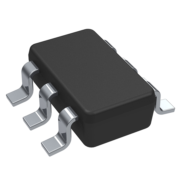
TLV9041SIDBVR

Why Choose Us?
Professional Platform
B2B & B2C purchasingDelivery at full speed
1-2 days deliveryWide variety
Original manufacturers365 days guarantee
Responsible quality
.png)


Tech Specifications
TLV9041SIDBVR Description
The TLV9041SIDBVR is a low-power, high-accuracy analog-to-digital converter (ADC) from Texas Instruments. It is designed for use in a variety of applications, including industrial, medical, and consumer electronics.
Description:
The TLV9041SIDBVR is a 12-bit SAR ADC that operates from a single 2.7V to 5.5V supply. It features a low power consumption of only 85µA, making it ideal for battery-powered applications. The device has a small 10-pin WSON package, making it suitable for space-constrained applications.
Features:
- 12-bit resolution
- Single 2.7V to 5.5V supply
- Low power consumption of 85µA
- Small 10-pin WSON package
- Input voltage range of 0V to 3.3V
- Sampling rate of up to 200ksps
- Programmable gain amplifier (PGA) with four gain settings
- I2C interface for easy integration with microcontrollers
- Internal reference of 1.2V or 2.5V
- Low noise and high accuracy
Applications:
The TLV9041SIDBVR is suitable for a wide range of applications, including:
- Industrial control systems
- Medical equipment
- Battery-powered devices
- Consumer electronics
- IoT devices
- Data acquisition systems
- Power monitoring systems
- Temperature sensing
- Strain gauge measurement
In summary, the TLV9041SIDBVR is a low-power, high-accuracy ADC that is ideal for use in a variety of applications. Its small size and low power consumption make it well-suited for battery-powered devices, while its high accuracy and low noise make it suitable for precision measurement applications.
FAQ
| Quantity | Unit Price | Ext. Price |
|---|---|---|
| 1+ | $0.47315 | $0.47 |
| 10+ | $0.46115 | $4.61 |
| 30+ | $0.45257 | $13.58 |
Not available to buy online? Want the lower wholesale price? Please Send RFQ to get best price, we will respond immediately


.png?x-oss-process=image/format,webp/resize,h_32)


