
Texas Instruments
TLV9062IDGKT
OP Amps, Buffer Amps ICs


.png?x-oss-process=image/format,webp/resize,p_30)


TLV9062IDGKT Description
TLV9062IDGKT Description
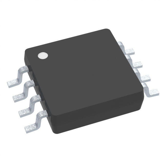
The TLV9062IDGKT is a high-performance CMOS operational amplifier from Texas Instruments, designed for a wide range of precision analog applications. This dual-channel amplifier is housed in an 8-pin VSSOP package, making it suitable for surface-mount applications where space is a premium. The TLV9062IDGKT operates from a supply voltage range of 1.8 V to 5.5 V, providing flexibility in various power supply configurations. With a gain bandwidth product of 10 MHz and a slew rate of 6.5 V/µs, this amplifier delivers excellent performance in both speed and precision.
TLV9062IDGKT Features
- Wide Supply Voltage Range: The TLV9062IDGKT operates from 1.8 V to 5.5 V, making it suitable for applications with varying power supply requirements.
- High Gain Bandwidth Product: With a gain bandwidth product of 10 MHz, this amplifier ensures high-frequency performance, ideal for applications requiring fast signal processing.
- Low Input Bias Current: The input bias current is as low as 0.5 pA, minimizing the impact on sensitive input signals and ensuring high accuracy.
- Low Input Offset Voltage: The voltage input offset is only 300 µV, contributing to high precision in signal amplification.
- High Output Current: Each channel can deliver up to 50 mA of output current, making it capable of driving demanding loads.
- Low Supply Current: The supply current is only 538 µA per channel, ensuring efficient power usage and minimal power dissipation.
- Compliance and Reliability: The TLV9062IDGKT is REACH unaffected and RoHS3 compliant, meeting environmental and safety standards. It also has a moisture sensitivity level (MSL) of 2 (1 year), ensuring reliability in various environmental conditions.
TLV9062IDGKT Applications
The TLV9062IDGKT is ideal for a variety of applications due to its high performance and versatility:
- Precision Signal Conditioning: Its low input bias current and low input offset voltage make it suitable for precision signal conditioning in sensor interfaces and analog front-ends.
- High-Speed Signal Processing: The 10 MHz gain bandwidth product and 6.5 V/µs slew rate enable high-speed signal processing in communication systems and data acquisition applications.
- Battery-Powered Devices: The wide supply voltage range and low supply current make it an excellent choice for battery-powered devices where power efficiency is critical.
- Industrial Control Systems: The high output current and robust performance make it suitable for industrial control systems requiring reliable and precise signal amplification.
Conclusion of TLV9062IDGKT
The TLV9062IDGKT from Texas Instruments is a versatile and high-performance CMOS operational amplifier that excels in precision and speed. Its wide supply voltage range, low input bias current, and high output current make it suitable for a wide range of applications, from precision signal conditioning to high-speed signal processing. The TLV9062IDGKT's compliance with environmental and safety standards ensures its reliability and suitability for modern electronics applications. Whether in battery-powered devices or industrial control systems, the TLV9062IDGKT stands out as a reliable and efficient choice for engineers and designers.
Tech Specifications
TLV9062IDGKT Documents
Download datasheets and manufacturer documentation for TLV9062IDGKT
 Additional Assembly Sites 16/Dec/2021
  Signal e-Book: OP Amp Design Topics TLV9061, 9062, 9064 Datasheet
  Marking change 01/Feb/2023
  TLV9061, 9062, 9064 Datasheet
  TLV9061/TLV9062/TLV9064 08/Oct/2019
 Shopping Guide


.png?x-oss-process=image/format,webp/resize,h_32)


