
Texas Instruments
TMS320F2812GBBAR
DSP


.png?x-oss-process=image/format,webp/resize,p_30)


TMS320F2812GBBAR Description
TMS320F2812GBBAR Description
The TMS320F2812GBBAR is a high-performance microcontroller unit (MCU) from Texas Instruments, designed for demanding embedded applications in the automotive industry. This MCU features a robust architecture with a 150MHz clock rate, ensuring rapid processing capabilities. It is equipped with 256kB of FLASH non-volatile memory and 36kB of on-chip RAM, providing ample storage for complex algorithms and data retention. The device operates with a core voltage of 1.9V and an I/O voltage of 3.30V, ensuring efficient power management and compatibility with various peripheral devices.
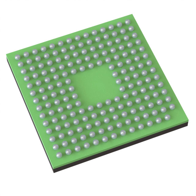
The TMS320F2812GBBAR is packaged in a surface-mount format, specifically in a Tape & Reel (TR) configuration, which facilitates automated assembly processes and enhances reliability in automotive environments. It is rated for automotive grade applications, ensuring it meets the stringent standards required for safety-critical systems. The device is currently active in production, with an ECCN classification of 3A991A2 and an HTSUS code of 8542.31.0001. It has a moisture sensitivity level (MSL) of 3, allowing for a 168-hour exposure period, making it suitable for various manufacturing processes.
TMS320F2812GBBAR Features
The TMS320F2812GBBAR offers a comprehensive set of features that set it apart from similar models. Its floating-point type architecture enables precise calculations, crucial for applications requiring high accuracy. The MCU supports multiple interfaces, including CAN, EBI/EMI, McBSP, SCI, SPI, and UART, providing extensive connectivity options for interfacing with various sensors, actuators, and communication networks.
One of the unique advantages of the TMS320F2812GBBAR is its combination of high memory capacity and processing speed. The 256kB FLASH memory allows for the storage of complex firmware and data, while the 36kB on-chip RAM ensures fast access to frequently used data, reducing latency and enhancing overall system performance. The 150MHz clock rate ensures that the MCU can handle real-time processing tasks efficiently, making it ideal for time-sensitive applications.
TMS320F2812GBBAR Applications
The TMS320F2812GBBAR is particularly well-suited for automotive applications due to its automotive grade rating and robust performance. It is ideal for use in engine control units (ECUs), where precise control and real-time processing are critical. The MCU's extensive interface capabilities make it suitable for integrating with various automotive sensors and systems, such as anti-lock braking systems (ABS), electronic stability control (ESC), and advanced driver-assistance systems (ADAS).
Beyond automotive applications, the TMS320F2812GBBAR can be employed in industrial control systems, where its high processing speed and memory capacity are beneficial for managing complex automation tasks. Its floating-point architecture also makes it suitable for applications in scientific instrumentation and medical devices, where precision and reliability are paramount.
Conclusion of TMS320F2812GBBAR
In summary, the TMS320F2812GBBAR from Texas Instruments is a versatile and high-performance MCU tailored for demanding embedded applications. Its combination of a 150MHz clock rate, 256kB FLASH memory, and 36kB on-chip RAM, along with its extensive interface options, make it a powerful solution for automotive and industrial applications. The device's automotive grade rating and surface-mount packaging ensure reliability and compatibility with modern manufacturing processes. Whether used in engine control units, industrial automation systems, or precision instruments, the TMS320F2812GBBAR delivers the performance and features necessary to meet the demands of today's complex embedded systems.
Tech Specifications
TMS320F2812GBBAR Documents
Download datasheets and manufacturer documentation for TMS320F2812GBBAR
 TMS320F281x
 Relevant Search
Shopping Guide


.png?x-oss-process=image/format,webp/resize,h_32)


