
 German
 Japanese
 Portuguese
 Korea
Korea
 Mexico
 Dutch
Dutch


Texas Instruments
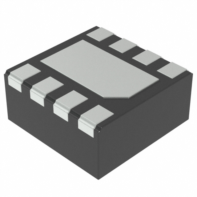
TPS22965QWDSGTQ1

Why Choose Us?
Professional Platform
B2B & B2C purchasingDelivery at full speed
1-2 days deliveryWide variety
Original manufacturers365 days guarantee
Responsible quality
.png)


Tech Specifications
TPS22965QWDSGTQ1 Description
The TPS22965QWDSGTQ1 is a high-performance, fully integrated power management solution from Texas Instruments (TI). This device is designed to provide efficient and reliable power conversion for a wide range of applications, including industrial, medical, and telecom equipment.
Description:
The TPS22965QWDSGTQ1 is a highly integrated, high-efficiency step-down (buck) regulator that can accept a wide input voltage range of 4.75V to 60V. It is available in a compact 16-lead QFN (3x3mm) package, making it suitable for space-constrained applications.
Features:
- Wide input voltage range: 4.75V to 60V
- High efficiency: Up to 95% efficiency, depending on the input voltage and output current
- Programmable output voltage: Adjustable output voltage from 0.8V to 5.5V using an external resistor
- High output current: Capable of delivering up to 3A of continuous output current
- Small form factor: 16-lead QFN package (3x3mm)
- Low quiescent current: 3.5µA in normal operation mode and 1µA in power save mode
- Integrated high-side and low-side MOSFETs
- Soft-start and over-current protection
- Thermal shutdown and over-temperature warning
- Spread spectrum frequency modulation for reduced electromagnetic interference (EMI)
Applications:
- Industrial control systems
- Medical equipment, such as portable medical devices and patient monitoring systems
- Telecommunication equipment, including base stations, routers, and switches
- Networking devices, such as Ethernet switches and Wi-Fi access points
- Battery-powered devices, including portable electronics and IoT devices
- LED lighting systems
- General-purpose power conversion in various electronic devices
The TPS22965QWDSGTQ1 is a versatile and efficient power management solution that can be used in a wide range of applications requiring a compact, high-performance step-down regulator. Its wide input voltage range, high efficiency, and programmable output voltage make it suitable for various power conversion needs.
FAQ
| Quantity | Unit Price | Ext. Price |
|---|---|---|
| 5+ | $0.39085 | $1.95 |
| 50+ | $0.30343 | $15.17 |
| 250+ | $0.26743 | $66.86 |
Not available to buy online? Want the lower wholesale price? Please Send RFQ to get best price, we will respond immediately


.png?x-oss-process=image/format,webp/resize,h_32)


