
Texas Instruments
TPS60302DGS
DC Switching Voltage Regulators


.png?x-oss-process=image/format,webp/resize,p_30)


TPS60302DGS Description
TPS60302DGS Description
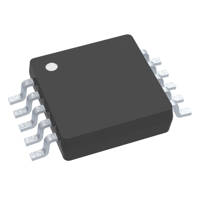
The TPS60302DGS is a fixed output voltage charge pump regulator designed for high efficiency and low power consumption. Manufactured by Texas Instruments, this device is part of the Power Management Integrated Circuit (PM)IC category, specifically tailored for applications requiring a reliable and efficient power solution. The TPS60302DGS features a fixed output voltage configuration, providing two positive outputs with a minimum fixed voltage of 2Vin and 3.3V. It operates within an input voltage range of 0.9V to 1.8V, making it suitable for low-voltage applications. The device can deliver output currents of up to 40mA and 20mA, respectively, ensuring robust performance in various electronic systems.
TPS60302DGS Features
- Efficient Charge Pump Topology: Utilizing a charge pump topology, the TPS60302DGS achieves high efficiency and low quiescent current, making it ideal for battery-powered and low-power applications.
- Wide Input Voltage Range: With an input voltage range of 0.9V to 1.8V, the TPS60302DGS can operate effectively in systems with varying input voltages, ensuring reliable performance.
- High Output Current Capability: The device supports output currents of up to 40mA and 20mA, providing sufficient power for multiple loads.
- Fixed Output Voltage: The fixed output voltage of 2Vin and 3.3V simplifies design and ensures stable power delivery to connected devices.
- High Switching Frequency: Operating at a switching frequency of 700kHz, the TPS60302DGS minimizes the size of external components, reducing the overall footprint of the power supply.
- Surface Mount Packaging: The TPS60302DGS is available in a surface mount package, facilitating easy integration into compact and high-density PCB designs.
- Compliance and Reliability: The device is REACH unaffected and RoHS3 compliant, ensuring environmental safety and regulatory compliance. Additionally, its Moisture Sensitivity Level (MSL) is 1 (Unlimited), making suitable it for various manufacturing environments.
TPS60302DGS Applications
The TPS60302DGS is well-suited for a variety of applications where efficient power management is critical. Some specific use cases include:
- Battery-Powered Devices: Ideal for portable electronics such as smartphones, tablets, and wearables, where low power consumption and high efficiency are essential.
- Low-Voltage Systems: Suitable for applications with low input voltage requirements, such as IoT devices and sensors, ensuring reliable operation even in low-power environments.
- Multiple Load Applications: With two positive outputs, the TPS60302DGS can power multiple devices or components simultaneously, simplifying power distribution in complex systems.
- Space-Constrained Designs: The surface mount package and high switching frequency allow for compact and efficient power supply designs, making it perfect for applications with limited board space.
Conclusion of TPS60302DGS
The TPS60302DGS from Texas Instruments is a robust and efficient charge pump regulator designed for low-voltage, low-power applications. Its wide input voltage range, high output current capability, and fixed output voltage make it a versatile solution for various electronic systems. The device's high switching frequency and surface mount packaging further enhance its suitability for compact and high-density designs. With its compliance to environmental and regulatory standards, the TPS60302DGS ensures reliable performance and ease of integration into modern electronic devices.
Tech Specifications
TPS60302DGS Documents
Download datasheets and manufacturer documentation for TPS60302DGS
 Product Discontinuance Notification 2024-07-01 (PDF) Product Discontinuance Notification (PDF)
  Mechanical Outline Drawing
  TPS60302DGS Symbol & Footprint by SnapMagic
 Shopping Guide


.png?x-oss-process=image/format,webp/resize,h_32)


