

Not available to buy online? Want the lower wholesale price? Please Send RFQ to get best price, we will respond immediately


.png?x-oss-process=image/format,webp/resize,p_30)


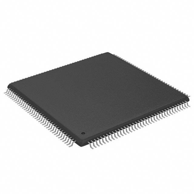
XC2S50-5TQ144C Description
AMD's XC2S50-5TQ144C is a high-performance, low-power, and versatile programmable logic device designed for a wide range of applications. This device is part of the Xilinx CoolRunner-II series, which is known for its low power consumption and high integration capabilities.
Description:
The XC2S50-5TQ144C is a surface-mount Field Programmable Gate Array (FPGA) that features a programmable logic array, configurable I/O, and other essential components. It is housed in a 144-pin Thin Quad Flat Package (TQFP) and operates at a maximum frequency of 100 MHz.
Features:
- Low power consumption: The device is designed to consume minimal power, making it suitable for battery-powered and energy-sensitive applications.
- High integration: The XC2S50-5TQ144C offers a high level of integration, allowing for the implementation of complex designs in a compact form factor.
- Versatile I/O: The device features a wide range of configurable I/O options, including LVCMOS, LVDS, and others, making it suitable for various interface requirements.
- On-chip memory: The FPGA includes on-chip memory resources, such as block RAM and distributed RAM, for efficient data storage and processing.
- High-performance logic elements: The XC2S50-5TQ144C is equipped with high-performance logic elements that can be configured to implement a wide range of digital logic functions.
- JTAG programming: The device supports JTAG (Joint Test Action Group) programming, allowing for easy and flexible reprogramming of the device.
Applications:
The XC2S50-5TQ144C is suitable for a wide range of applications, including but not limited to:
- Industrial control systems: The device can be used in industrial control systems for implementing complex logic functions and interfacing with various sensors and actuators.
- Communication systems: The versatile I/O options and high-performance logic elements make the XC2S50-5TQ144C suitable for communication systems, such as serial communication interfaces and network controllers.
- Consumer electronics: The low power consumption and compact form factor of the XC2S50-5TQ144C make it ideal for use in battery-powered consumer electronics, such as portable devices and wearables.
- Automotive systems: The device can be used in automotive systems for implementing safety-critical functions and interfacing with various sensors and actuators.
- Medical devices: The XC2S50-5TQ144C can be used in medical devices for implementing complex signal processing algorithms and interfacing with various medical sensors and instruments.
In summary, the AMD XC2S50-5TQ144C is a versatile, low-power, and high-performance FPGA that offers a wide range of features and applications. Its compact form factor, low power consumption, and flexible I/O options make it suitable for a variety of applications, from industrial control systems to consumer electronics.
Tech Specifications
XC2S50-5TQ144C Documents
Download datasheets and manufacturer documentation for XC2S50-5TQ144C
 Mult Dev LeadFrame Chg 29/Oct/2018 Spartan-II FPGA Family Mult DEV EOL 01/Jan/2024 Xilinx REACH211 Cert Xiliinx RoHS Cert
 Related Parts


Relevant Search
Shopping Guide


.png?x-oss-process=image/format,webp/resize,h_32)


©2025 ERSA Electronics Corporation.