

Not available to buy online? Want the lower wholesale price? Please Send RFQ to get best price, we will respond immediately


.png?x-oss-process=image/format,webp/resize,p_30)


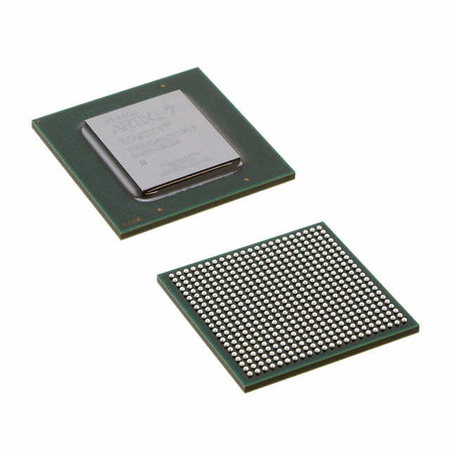
XC7A200T-1FB676I Description
XC7A200T-1FB676I Overview
There are 215360 logic elements or cells that make up a fundamental building block. With your development board connected through the Surface Mount connection, you may utilize this FPGA module. The device operates between 0.95V and 1.05V, which is its supply voltage. It's crucial to maintain the machine's temperature within the -40°C to 100°C TJ range while it's in operation. This FPGA model is packed in Tray for space-saving purposes. This device will provide you with a lot of memory thanks to its RAM bit size of 13455360. This FPGA should function flawlessly if put in Surface Mount, according to its specs. When using its full power, this module can operate at temperatures as high as 100°C.
XC7A200T-1FB676I Features
High-speed serial connectivity with built-in multi-gigabit transceivers from 600 Mb/s to max rates of 6.6 Gb/s up to 28.05 Gb/s, offering a special low-power mode, optimized for chip-to-chip interfaces.
A user-configurable analog interface (XADC), incorporating dual 12-bit 1MSPS analog-to-digital converters with on-chip thermal and supply sensors.
Powerful clock management tiles (CMT), combining phase-locked loop (PLL) and mixed-mode clock manager (MMCM) blocks for high precision and low jitter.
Quickly deploy embedded processing with MicroBlaze™ processor.
Integrated block for PCI Express® (PCIe), for up to x8 Gen3
Endpoint and Root Port designs
XC7A200T-1FB676I Applications
Industrial Control
Internet of Things
Medical Equipment
Consumer Electronics
Aerospace & Defense
Tech Specifications
XC7A200T-1FB676I Documents
Download datasheets and manufacturer documentation for XC7A200T-1FB676I
 XC7A100T/200T Errata 7 Series FPGA Overview Artix-7 FPGAs Datasheet Artix-7 FPGAs Brief Mult Dev Material Chg 16/Dec/2019 Cross-Ship Lead-Free Notice 31/Oct/2016 Xilinx REACH211 Cert Xiliinx RoHS Cert
 Related Parts


Relevant Search
Shopping Guide


.png?x-oss-process=image/format,webp/resize,h_32)


©2025 ERSA Electronics Corporation.