
 German
 Japanese
 Portuguese
 Korea
Korea
 Mexico
 Dutch
Dutch


Why Choose Us?
Professional Platform
B2B & B2C purchasingDelivery at full speed
1-2 days deliveryWide variety
Original manufacturers365 days guarantee
Responsible quality
.png)


Tech Specifications
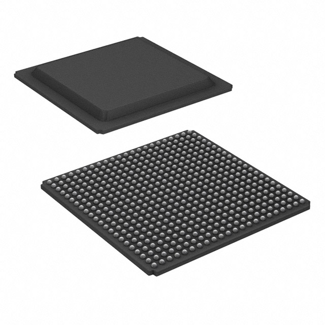
XC7S50-2FGGA484C Description
XC7S50-2FGGA484C Overview
250 I/Os allow data to be transported more efficiently. 52160 logic elements/cells make up logic blocks. A voltage source of 1V volts is required to run FPGA chips. This FPGA module can be connected to the development board through a Surface Mount connector—a battery of 0.95V1.05V powers this device. FPGA chips are required to keep the operational temperature between 0°C and 85°C TJ when the device is turned on. Unlike previous FPGA variants, this one is confined within Tray to save space. It contains 484 terminations in all. It is worth noting that this device comes with 2764800 FPGA electronics s of RAM.
XC7S50-2FGGA484C Features
A user-configurable analogue interface (XADC), incorporating dual 12-bit 1MSPS analogue-to-digital converters with on-chip thermal and supply sensors.
Powerful clock management tiles (CMT), combining phase-locked loop (PLL) and mixed-mode clock manager (MMCM) blocks for high precision and low jitter.
Quickly deploy embedded processing with MicroBlaze™ processor.
XC7S50-2FGGA484C Applications
Wireless Communications
Voice recognition
Embedded Vision
Audio
Enterprise networking
FAQ
| Quantity | Unit Price | Ext. Price |
|---|---|---|
| 1+ | $30.91885 | $30.92 |
| 30+ | $29.58515 | $887.55 |
Not available to buy online? Want the lower wholesale price? Please Send RFQ to get best price, we will respond immediately


.png?x-oss-process=image/format,webp/resize,h_32)


