
 German
 Japanese
 Portuguese
 Korea
Korea
 Mexico
 Dutch
Dutch


Infineon Technologies
BSP296NH6327XTSA1

Why Choose Us?
Professional Platform
B2B & B2C purchasingDelivery at full speed
1-2 days deliveryWide variety
Original manufacturers365 days guarantee
Responsible quality
.png)


Tech Specifications
BSP296NH6327XTSA1 Description
BSP296NH6327XTSA1 Description
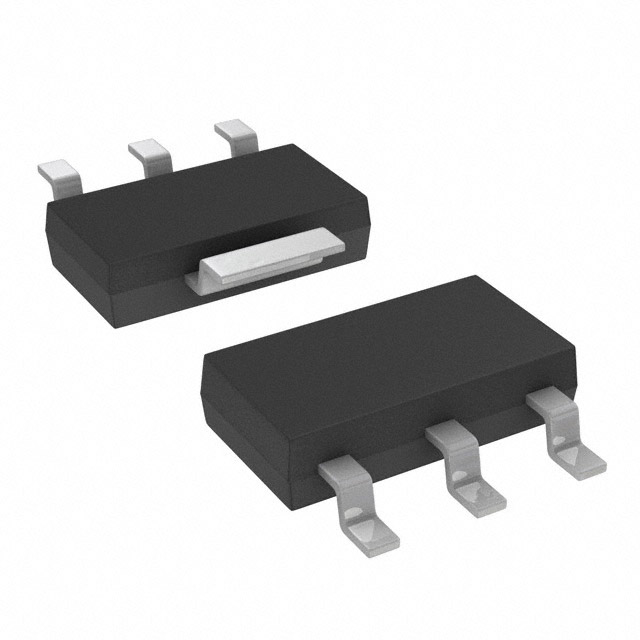
The BSP296NH6327XTSA1 from Infineon Technologies is a high-performance N-channel MOSFET designed for efficient power management in compact, surface-mount applications. Part of the OptiMOS™ series, this device offers a 100V drain-to-source voltage (Vdss) rating and a continuous drain current (Id) of 1.2A at 25°C, making it suitable for low-to-medium power switching applications. With an Rds(on) as low as 600mΩ at 10V gate drive, it ensures minimal conduction losses, enhancing energy efficiency. The MOSFET operates within a gate-source voltage (Vgs) range of ±20V and features a low gate threshold voltage (Vgs(th)) of 1.8V, enabling compatibility with low-voltage control circuits. Packaged in SOT223-4 and supplied in Tape & Reel (TR), it is optimized for automated assembly processes.
BSP296NH6327XTSA1 Features
- Low Gate Charge (Qg): 6.7 nC @ 10V reduces switching losses, improving high-frequency performance.
- Low Input Capacitance (Ciss): 152.7 pF @ 25V minimizes drive requirements and enhances switching speed.
- High Efficiency: Optimized Rds(on) and Qg balance ensures superior power handling with minimal heat generation.
- Robust Construction: ROHS3 Compliant and REACH Unaffected, meeting stringent environmental and safety standards.
- Wide Operating Range: 4.5V to 10V gate drive flexibility suits both logic-level and standard MOSFET drivers.
- Reliability: MSL 1 (Unlimited) moisture sensitivity ensures long shelf life and handling ease.
BSP296NH6327XTSA1 Applications
This MOSFET is ideal for:
- DC-DC Converters: Efficient power conversion in portable devices and industrial power supplies.
- Load Switching: Low-loss switching in battery management systems (BMS) and power distribution circuits.
- Motor Control: Compact driver solutions for small motors in automotive and consumer electronics.
- LED Drivers: High-efficiency dimming and control in lighting applications.
- Power Management ICs (PMICs): Integration into space-constrained designs requiring reliable switching performance.
Conclusion of BSP296NH6327XTSA1
The BSP296NH6327XTSA1 stands out for its low Rds(on), fast switching, and compact SOT223-4 package, making it a versatile choice for modern power electronics. Its OptiMOS™ technology ensures high efficiency and thermal performance, while its wide Vgs range and low gate charge cater to diverse control requirements. Whether used in DC-DC conversion, motor drives, or LED systems, this MOSFET delivers reliable performance with minimal losses, aligning with the demands of energy-efficient and high-density designs.
FAQ
Not available to buy online? Want the lower wholesale price? Please Send RFQ to get best price, we will respond immediately


.png?x-oss-process=image/format,webp/resize,h_32)


