
 German
 Japanese
 Portuguese
 Korea
Korea
 Mexico
 Dutch
Dutch


Intel
EP2C35F484I8N

Why Choose Us?
Professional Platform
B2B & B2C purchasingDelivery at full speed
1-2 days deliveryWide variety
Original manufacturers365 days guarantee
Responsible quality
.png)


Tech Specifications
EP2C35F484I8N Description
EP2C35F484I8N Description
The EP2C35F484I8N is an advanced Field Programmable Gate Array (FPGA) from Intel, part of the Cyclone® II series. This device is designed for high-performance embedded applications requiring significant computational power and flexibility. With a total of 483,840 RAM bits and 33,216 logic elements/cells, the EP2C35F484I8N offers substantial memory and processing capabilities. It features 2,076 Logic Array Blocks/Configurable Logic Blocks (LABs/CLBs) and supports up to 322 I/O pins, making it highly versatile for complex system designs.
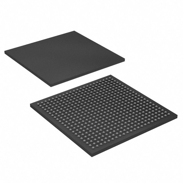
The EP2C35F484I8N operates within a supply voltage range of 1.15V to 1.25V, ensuring efficient power usage and thermal management. Its surface-mount technology (SMT) and 484-pin Fine Ball Grid Array (FBGA) package make it suitable for compact and high-density PCB layouts. The device is available in tray packaging and has a moisture sensitivity level (MSL) of 3, allowing for a 168-hour exposure time before assembly.
EP2C35F484I8N Features
- High Memory Capacity: With 483,840 RAM bits, the EP2C35F484I8N provides ample memory for storing data and instructions, essential for complex algorithms and data processing tasks.
- Robust Logic Elements: The 33,216 logic elements/cells allow for the implementation of sophisticated digital circuits and systems, supporting a wide range of applications from signal processing to control systems.
- Extensive I/O Capability: The 322 I/O pins offer extensive connectivity options, making it suitable for interfacing with various peripherals and external devices.
- Power Efficiency: The operating voltage range of 1.15V to 1.25V ensures low power consumption, which is critical for battery-powered and energy-efficient designs.
- Compliance and Reliability: The EP2C35F484I8N is RoHS compliant and REACH unaffected, ensuring it meets environmental and safety standards. The device is also categorized under ECCN 3A991D and HTSUS 8542.39.0001, facilitating international trade and regulatory compliance.
EP2C35F484I8N Applications
The EP2C35F484I8N is ideal for a variety of high-performance embedded applications, including:
- Telecommunications: For baseband processing, signal modulation, and demodulation in wireless communication systems.
- Consumer Electronics: In high-definition video processing, digital signal processing for audio and video applications, and smart home automation systems.
- Industrial Control: For real-time control systems, automation, and robotics where precise and rapid processing is required.
- Medical Devices: In medical imaging systems, patient monitoring devices, and diagnostic equipment where reliability and performance are paramount.
Conclusion of EP2C35F484I8N
The EP2C35F484I8N is a powerful and versatile FPGA from Intel, offering a combination of high memory capacity, robust logic elements, and extensive I/O capabilities. Its power efficiency, compliance with environmental standards, and reliable performance make it a preferred choice for demanding embedded applications. Whether used in telecommunications, consumer electronics, industrial control, or medical devices, the EP2C35F484I8N stands out for its ability to deliver high performance in a compact and energy-efficient package.
FAQ
Not available to buy online? Want the lower wholesale price? Please Send RFQ to get best price, we will respond immediately


.png?x-oss-process=image/format,webp/resize,h_32)


