
 German
 Japanese
 Portuguese
 Korea
Korea
 Mexico
 Dutch
Dutch


Lattice Semiconductor
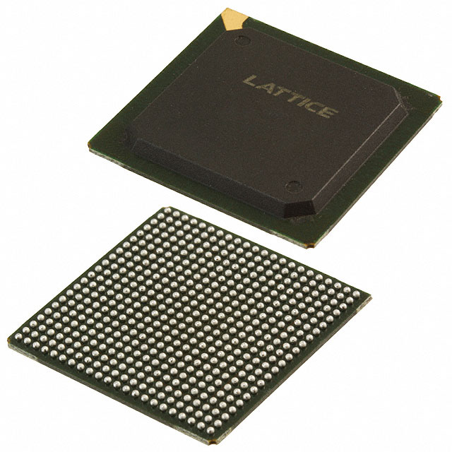
LCMXO2-2000UHC-4FG484C

Why Choose Us?
Professional Platform
B2B & B2C purchasingDelivery at full speed
1-2 days deliveryWide variety
Original manufacturers365 days guarantee
Responsible quality
.png)


Tech Specifications
LCMXO2-2000UHC-4FG484C Description
The Lattice Semiconductor's LCMXO2-2000UHC-4FG484C is a high-performance field programmable gate array (FPGA) device that is designed to meet the demands of various applications in the electronics industry.
Description:
The LCMXO2-2000UHC-4FG484C is an ultra-high performance, low power FPGA that is based on the company's 28 nm technology. It features a high-density architecture that provides a large number of programmable logic elements, digital signal processing blocks, and memory resources. The device is available in a 484-ball fine pitch ball grid array (FBGA) package, making it suitable for use in a wide range of applications.
Features:
Some of the key features of the LCMXO2-2000UHC-4FG484C include:
- High-performance programmable logic with low power consumption
- A wide range of I/O options for flexible system integration
- Advanced digital signal processing capabilities for demanding applications
- High-density memory resources for data storage and processing
- Security features for protecting intellectual property and system integrity
- A comprehensive development toolset for easy design and implementation
Applications:
The LCMXO2-2000UHC-4FG484C is suitable for a wide range of applications, including:
- Communications infrastructure, such as routers, switches, and network interface cards
- Industrial control systems, such as motor control and machine vision
- Automotive systems, such as advanced driver assistance systems (ADAS) and infotainment systems
- Consumer electronics, such as set-top boxes, gaming consoles, and smart home devices
- Aerospace and defense systems, such as radar and electronic warfare systems
Overall, the LCMXO2-2000UHC-4FG484C is a versatile and powerful FPGA that offers high performance, low power consumption, and a wide range of features that make it suitable for a variety of applications in the electronics industry.
FAQ
Not available to buy online? Want the lower wholesale price? Please Send RFQ to get best price, we will respond immediately


.png?x-oss-process=image/format,webp/resize,h_32)


