

Lattice Semiconductor
LCMXO2-256HC-4SG32C
FPGAs

Not available to buy online? Want the lower wholesale price? Please Send RFQ to get best price, we will respond immediately


.png?x-oss-process=image/format,webp/resize,p_30)


LCMXO2-256HC-4SG32C Description
LCMXO2-256HC-4SG32C Description
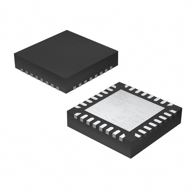
The LCMXO2-256HC-4SG32C is a high-performance Field Programmable Gate Array (FPGA) from Lattice Semiconductor, a leading provider of innovative silicon solutions. This device is part of the MachXO2 series, known for its versatility and efficiency in embedded applications. The LCMXO2-256HC-4SG32C is designed for surface mount applications and comes in a 32QFN package, making it suitable for compact and space-constrained designs.
This FPGA features 256 logic elements/cells and 32 Logic Array Blocks (LABs)/Configurable Logic Blocks (CLBs), providing ample resources for complex digital designs. It supports a wide operating temperature range of 0°C to 85°C (TJ), ensuring reliable performance in various environmental conditions. The device operates within a supply voltage range of 2.375V to 3.465V, offering flexibility in power supply options.
With 21 I/O pins, the LCMXO2-256HC-4SG32C can interface with a variety of external devices, making it ideal for applications requiring extensive connectivity. The device is RoHS3 compliant and REACH unaffected, ensuring it meets the highest environmental and regulatory standards. The moisture sensitivity level (MSL) is rated at 3 (168 hours), making it suitable for manufacturing processes that require moisture protection.
LCMXO2-256HC-4SG32C Features
- High Logic Capacity: With 256 logic elements/cells and 32 LABs/CLBs, the LCMXO2-256HC-4SG32C offers significant logic capacity, enabling the implementation of complex digital circuits and algorithms.
- Wide Operating Temperature Range: The device operates reliably within a temperature range of 0°C to 85°C (TJ), making it suitable for industrial and consumer applications in diverse environments.
- Flexible I/O Options: The 21 I/O pins provide extensive connectivity options, allowing the FPGA to interface with various external devices and peripherals.
- Wide Supply Voltage Range: The device supports a supply voltage range of 2.375V to 3.465V, offering flexibility in power supply design.
- Compliance and Reliability: The LCMXO2-256HC-4SG32C is RoHS3 compliant and REACH unaffected, ensuring it meets stringent environmental and regulatory standards. The MSL rating of 3 (168 hours) ensures reliability during manufacturing processes.
- Surface Mount Packaging: The 32QFN package is ideal for surface mount applications, providing a compact and efficient solution for space-constrained designs.
LCMXO2-256HC-4SG32C Applications
The LCMXO2-256HC-4SG32C is well-suited for a variety of applications due to its high logic capacity, flexible I/O options, and wide operating temperature range. Some specific use cases include:
- Consumer Electronics: Ideal for applications requiring complex digital processing and extensive connectivity, such as smart home devices, gaming consoles, and multimedia systems.
- Industrial Automation: Suitable for industrial control systems, where the device can manage complex logic operations and interface with various sensors and actuators.
- Telecommunications: The FPGA can be used in communication systems for signal processing, protocol conversion, and other digital tasks.
- Automotive: The wide operating temperature range and robustness make it suitable for automotive applications, such as engine control units and advanced driver-assistance systems (ADAS).
Conclusion of LCMXO2-256HC-4SG32C
The LCMXO2-256HC-4SG32C is a versatile and high-performance FPGA from Lattice Semiconductor, offering significant logic capacity and flexible I/O options. Its wide operating temperature range and compliance with environmental standards make it a reliable choice for various applications. Whether used in consumer electronics, industrial automation, telecommunications, or automotive systems, the LCMXO2-256HC-4SG32C provides a robust and efficient solution for complex digital designs.
Tech Specifications
LCMXO2-256HC-4SG32C Documents
Download datasheets and manufacturer documentation for LCMXO2-256HC-4SG32C
Alternate Qualified Test Site 30/Sep/2013 MachXO2 Family Datasheet MachXO2 Family Handbook Leaded Pkg PCB Layout Guide All Dev Pkg Mark Chg 12/Nov/2018 MachXO2 Family Handbook MachXO2™ Family Datasheet MachXO2 Family Datasheet 30/Sep/2013 Top Mark Format Change 20/Dec/2023 Related Parts


Relevant Search
Shopping Guide


.png?x-oss-process=image/format,webp/resize,h_32)


©2025 ERSA Electronics Corporation.