Lattice Semiconductor
LCMXO2-256ZE-3SG32I
FPGAs


.png?x-oss-process=image/format,webp/resize,p_30)


LCMXO2-256ZE-3SG32I Description
The Lattice Semiconductor's LCMXO2-256ZE-3SG32I is a high-performance field programmable gate array (FPGA) that offers a wide range of features and applications. Here is a description of the model, its features, and potential applications:
Description:
The LCMXO2-256ZE-3SG32I is a member of Lattice Semiconductor's low-cost, low-power, and versatile ECP5 FPGA family. It is a mid-range device that provides a good balance between performance, power consumption, and cost. The part number indicates that it has 256 macrocells, a -3 speed grade, and is available in a 32-lead small-outline package (SOIC).
Features:
- Low Power Consumption: The LCMXO2-256ZE-3SG32I is designed to offer low power consumption, making it suitable for battery-powered and energy-sensitive applications.
- High Performance: With its 256 macrocells, the device provides a good balance between performance and cost, making it suitable for a wide range of applications.
- Versatility: The ECP5 FPGA family is known for its versatility, allowing users to implement various digital logic functions and interfaces.
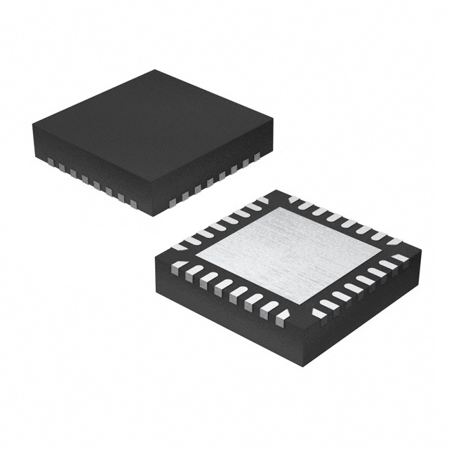
- Small Form Factor: The 32-lead SOIC package allows for compact designs, making it suitable for space-constrained applications.
- Field Programmability: As an FPGA, the LCMXO2-256ZE-3SG32I can be programmed and reprogrammed multiple times, providing flexibility in design and development.
- Wide Range of I/O Options: The device offers a variety of I/O options, including LVCMOS, LVDS, and others, allowing for easy integration with other components and systems.
Applications:
- Industrial Control Systems: The LCMXO2-256ZE-3SG32I can be used in industrial control systems for implementing custom logic functions, interfacing with sensors and actuators, and managing communication protocols.
- Consumer Electronics: The low power consumption and small form factor make it suitable for use in battery-powered consumer electronics, such as portable devices and wearables.
- Communication Systems: The device can be used in communication systems for implementing custom communication protocols, managing data transfer, and interfacing with various communication standards.
- Automotive Systems: The LCMXO2-256ZE-3SG32I can be used in automotive systems for implementing custom control functions, managing communication between various subsystems, and interfacing with sensors and actuators.
- Medical Devices: The device can be used in medical devices for implementing custom logic functions, managing data acquisition and processing, and interfacing with various sensors and actuators.
- Security Systems: The FPGA can be used in security systems for implementing custom encryption and decryption algorithms, managing access control, and interfacing with various security devices.
In summary, the Lattice Semiconductor's LCMXO2-256ZE-3SG32I is a versatile, low-cost, and low-power FPGA that offers a wide range of features and applications. Its balance of performance, power consumption, and cost make it suitable for various industries and applications, including industrial control systems, consumer electronics, communication systems, automotive systems, medical devices, and security systems.
Tech Specifications
LCMXO2-256ZE-3SG32I Documents
Download datasheets and manufacturer documentation for LCMXO2-256ZE-3SG32I
 Alternate Qualified Test Site 30/Sep/2013
  MachXO2 Family Datasheet Product Selector Guide Leaded Pkg PCB Layout Guide
  All Dev Pkg Mark Chg 12/Nov/2018
  MachXO2™ Family Datasheet
  MachXO2 Family Datasheet 30/Sep/2013 Top Mark Format Change 20/Dec/2023
 Relevant Search
Shopping Guide


.png?x-oss-process=image/format,webp/resize,h_32)


