Lattice Semiconductor_LCMXO2-640HC-6SG48I

Lattice Semiconductor
LCMXO2-640HC-6SG48I  
FPGAs

LCMXO2-640HC-6SG48I
696-LCMXO2-640HC-6SG48I
Ersa
Lattice Semiconductor-LCMXO2-640HC-6SG48I-datasheets-8922961.pdf
IC FPGA 40 I/O 48QFN
In Stock : 3043

Not available to buy online? Want the lower wholesale price? Please Send RFQ to get best price, we will respond immediately

QUICK RFQ
ADD TO RFQ LIST
ersa FreeSample ersa flow
ISO9001
Quality Policy
ISO45001
ISO14001

LCMXO2-640HC-6SG48I Description
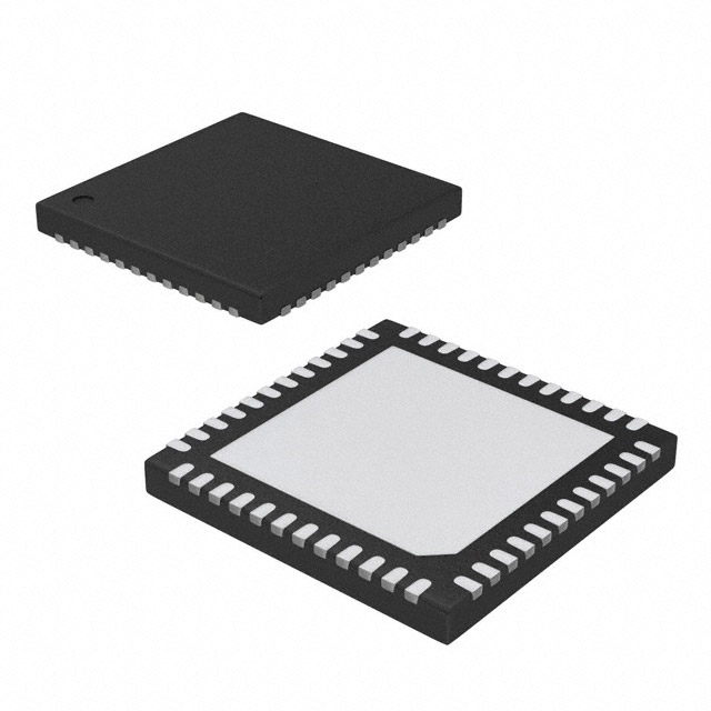
It is easier to move this LCMXO2-640HC-6SG48I and keep it dry by using this "Tray" packaging technique. This electronic component is produced by a company. Its goal is to increase the supply of high-performance chips and better meet consumer demand. An IC is a collection of electronic components -- resistors, transistors, capacitors, etc. All stuff into a tiny chip, and connected together to achieve a common goal. This Lattice Semiconductor's LCMXO2-640HC-6SG48I belongs to FPGAs category. And its FPGAs that falls under the category of Embedded IC Chips. This LCMXO2-640HC-6SG48I can function as an amplifier, oscillator, timer, counter, logic gate, computer memory, microcontroller or microprocessor. The cornerstone of all contemporary electronic gadgets is an integrated circuit (IC).

Tech Specifications

Program Memory Type
Logic Elements
PPAP
Product Status
Automotive
Total Number of Block RAM
Supplier Package
Device Logic Units
Number of I/O Banks
Package / Case
Voltage - Supply
REACH Status
Family Name
Maximum Operating Supply Voltage (V)
EU RoHS
Moisture Sensitivity Level (MSL)
Operating Temperature
Total RAM Bits
Number of LABs/CLBs
ECCN
Supplier Temperature Grade
Mounting Type
In-System Programmability
Standard Package Name
Pin Count
Reprogrammability Support
Mounting
HTSUS
Package
Speed Grade
User I/Os
Maximum Distributed RAM Bits
PCB changed
HTS
ECCN (US)
Supplier Device Package
Operating Supply Voltage (V)
Minimum Operating Temperature (°C)
Maximum Operating Temperature (°C)
Process Technology
Package Height
Mfr
Number of Logic Elements/Cells
I/O Voltage (V)
RoHS Status
Maximum Differential I/O Pairs
Number of I/O
Embedded Memory (Kbit)
Package Length
Series
Part Status
Package Width
Base Product Number
Shift Registers
Minimum Operating Supply Voltage (V)
Mounting Style
Unit Weight
Number of Logic Elements
Number of Logic Array Blocks - LABs
Embedded Memory
Adaptive Logic Modules - ALMs
RoHS
Supply Voltage - Min
Minimum Operating Temperature
Tradename
Moisture Sensitive
Operating Supply Voltage
Number of I/Os
Maximum Operating Frequency
Maximum Operating Temperature
Supply Voltage - Max
USHTS
Number of Transceivers

LCMXO2-640HC-6SG48I Documents

Download datasheets and manufacturer documentation for LCMXO2-640HC-6SG48I

Ersa MachXO2 Family Datasheet       MachXO2 Family Handbook       Package Diagrams      
Ersa All Dev Pkg Mark Chg 12/Nov/2018      
Ersa MachXO2 Family Handbook       MachXO2™ Family Datasheet      
Ersa Top Mark Format Change 20/Dec/2023      

Shopping Guide

Payment Methods
Payment Methods include Prepayment TT (bank transfer), Western Union, and PayPal. Customers are responsible for shipping costs, bank charges, customs duties and taxes.
Shipping Rate
Shipments are made once a day around 5pm, excluding Sundays. Once shipped, the estimated delivery time is usually 5-7 business days, depending on the courier you choose.
Delivery Methods
Provide DHL, FedEx, UPS, EMS, SF Express and Registered Airmail International Delivery Service