
 German
 Japanese
 Portuguese
 Korea
Korea
 Mexico
 Dutch
Dutch


Lattice Semiconductor
LCMXO2-640HC-6TG100I

Why Choose Us?
Professional Platform
B2B & B2C purchasingDelivery at full speed
1-2 days deliveryWide variety
Original manufacturers365 days guarantee
Responsible quality
.png)


Tech Specifications
LCMXO2-640HC-6TG100I Description
The Lattice Semiconductor's LCMXO2-640HC-6TG100I is a high-performance field programmable gate array (FPGA) that offers a wide range of features and applications. Here is a description of the model:
Description:
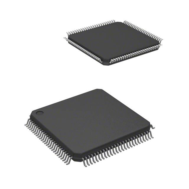
The LCMXO2-640HC-6TG100I is a member of the LatticeECP2 family of FPGAs. It is a mid-range device that provides a balance of power, performance, and cost-effectiveness. The device is available in a 6x6 mm TQFP package and operates over a wide range of supply voltages and temperatures.
Features:
- Low power consumption: The LCMXO2-640HC-6TG100I is designed for low power applications, making it ideal for battery-powered devices and systems with strict power budgets.
- High performance: The device offers high-speed performance with a maximum frequency of 640 MHz, making it suitable for demanding applications that require fast processing.
- Configurable logic blocks: The FPGA features a range of configurable logic blocks, including digital signal processing (DSP) slices, memory blocks, and I/O blocks, allowing for flexible and customizable designs.
- Embedded memory: The LCMXO2-640HC-6TG100I includes a variety of embedded memory options, such as block RAM and distributed RAM, to support complex data processing and storage requirements.
- High I/O count: The device offers a high number of I/O pins, providing connectivity options for various peripherals and interfaces.
- Security features: The FPGA includes security features such as encryption and authentication, ensuring the protection of sensitive data and intellectual property.
- RoHS compliant: The LCMXO2-640HC-6TG100I is compliant with the Restriction of Hazardous Substances (RoHS) directive, making it suitable for environmentally conscious applications.
Applications:
The LCMXO2-640HC-6TG100I is suitable for a wide range of applications, including:
- Industrial control systems: The device's low power consumption and high performance make it ideal for industrial control systems that require reliable and efficient operation.
- Consumer electronics: The FPGA's versatility and configurability make it suitable for various consumer electronics applications, such as smart home devices, wearables, and multimedia devices.
- Automotive systems: The LCMXO2-640HC-6TG100I can be used in automotive systems, such as infotainment systems, advanced driver assistance systems (ADAS), and body control modules.
- Networking and communication: The device's high-speed performance and I/O capabilities make it suitable for networking and communication applications, such as routers, switches, and base stations.
- Medical devices: The FPGA's low power consumption and security features make it suitable for medical devices that require reliable operation and data protection.
- Aerospace and defense: The LCMXO2-640HC-6TG100I can be used in aerospace and defense applications, such as satellite communication systems, radar systems, and navigation systems.
In summary, the Lattice Semiconductor's LCMXO2-640HC-6TG100I is a versatile and high-performance FPGA that offers a range of features suitable for various applications, including industrial control systems, consumer electronics, automotive systems, networking and communication, medical devices, and aerospace and defense.
FAQ
Not available to buy online? Want the lower wholesale price? Please Send RFQ to get best price, we will respond immediately


.png?x-oss-process=image/format,webp/resize,h_32)


