
 German
 Japanese
 Portuguese
 Korea
Korea
 Mexico
 Dutch
Dutch


Lattice Semiconductor
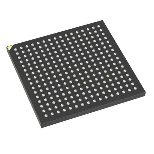
LCMXO2-7000HC-6BG256I

Why Choose Us?
Professional Platform
B2B & B2C purchasingDelivery at full speed
1-2 days deliveryWide variety
Original manufacturers365 days guarantee
Responsible quality
.png)


Tech Specifications
LCMXO2-7000HC-6BG256I Description
Lattice Semiconductor's LCMXO2-7000HC-6BG256I is a high-performance field programmable gate array (FPGA) device that offers a range of features and applications for various industries.
Description:
The LCMXO2-7000HC-6BG256I is a member of Lattice Semiconductor's low-cost, low-power, and small form factor FPGA family. It is based on the company's proprietary low-power 28 nm process technology and is designed to provide high performance and low power consumption in a compact package.
Features:
- High-performance 28 nm low-power process technology
- Small form factor package (6x6 mm BGA)
- Up to 7,000 logic elements (LEs)
- Up to 216 digital signal processing (DSP) slices
- Up to 112 megabits of block RAM (RAMB18)
- Up to 2,048 kilobits of distributed RAM (RAM4/RAM8)
- Support for high-speed I/O interfaces, including LVDS, DDR, and gigabit transceivers
- Integrated security features, including encryption and authentication
- Low power consumption, with power management features such as power-down modes and dynamic frequency scaling
- Comprehensive development tools and support, including Lattice Diamond software and IP cores
Applications:
The LCMXO2-7000HC-6BG256I is suitable for a wide range of applications that require high performance, low power consumption, and small form factor. Some potential applications include:
- Industrial control and automation systems
- Communication infrastructure, such as routers and switches
- Networking and data center equipment
- Consumer electronics, including set-top boxes and smart home devices
- Automotive systems, such as infotainment and advanced driver assistance systems (ADAS)
- Aerospace and defense applications, including communication and navigation systems
- Medical imaging and diagnostic equipment
- High-speed data acquisition and signal processing systems
- Machine vision and image processing applications
- IoT devices and edge computing platforms
In summary, the LCMXO2-7000HC-6BG256I is a versatile FPGA device that offers a combination of high performance, low power consumption, and small form factor, making it suitable for a wide range of applications across various industries.
FAQ
Not available to buy online? Want the lower wholesale price? Please Send RFQ to get best price, we will respond immediately


.png?x-oss-process=image/format,webp/resize,h_32)


