
 German
 Japanese
 Portuguese
 Korea
Korea
 Mexico
 Dutch
Dutch


Lattice Semiconductor
LFD2NX-17-8MG121C

Why Choose Us?
Professional Platform
B2B & B2C purchasingDelivery at full speed
1-2 days deliveryWide variety
Original manufacturers365 days guarantee
Responsible quality
.png)


Tech Specifications
LFD2NX-17-8MG121C Description
Lattice Semiconductor's LFD2NX-17-8MG121C is a high-performance field-programmable gate array (FPGA) device designed for a wide range of applications. This device is part of the CrossLink-NX family, which offers a combination of low power consumption, high performance, and small form factor.
Description:
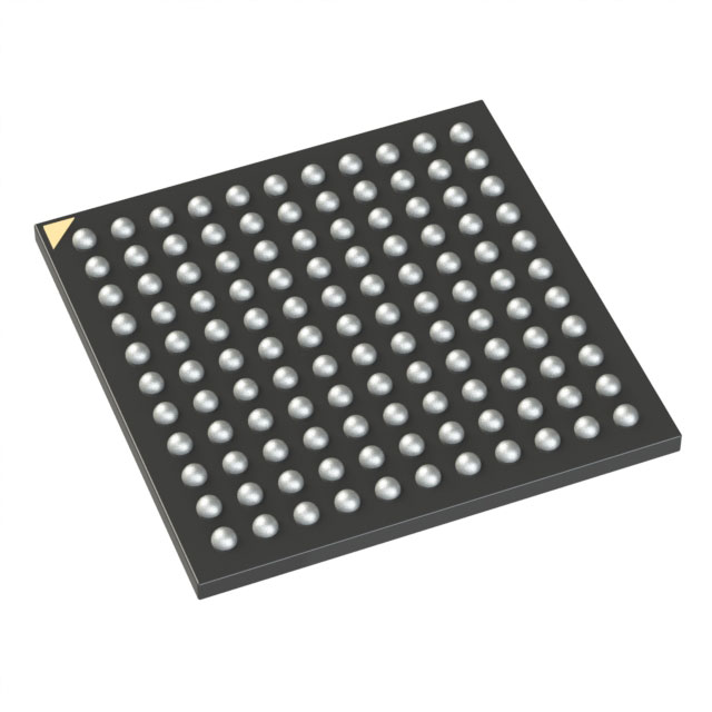
The LFD2NX-17-8MG121C is an FPGA device that features a 17 x 17 mm package size and a 121-ball fine-pitch ball grid array (FBGA). It is built using Lattice's advanced 28 nm low-power technology, which enables high performance and low power consumption.
Features:
- Low Power Consumption: The LFD2NX-17-8MG121C is designed for low power applications, making it suitable for battery-powered and energy-sensitive systems.
- High Performance: The device offers high-speed performance, with support for high-frequency clocking and fast I/O interfaces.
- Small Form Factor: With a compact 17 x 17 mm package size, the LFD2NX-17-8MG121C is ideal for space-constrained applications.
- Versatile I/O Options: The device supports a wide range of I/O standards, including LVDS, DDR, and MIPI, making it suitable for various interface requirements.
- Security Features: The LFD2NX-17-8MG121C includes advanced security features, such as encryption and authentication, to protect sensitive data and intellectual property.
- Easy Integration: The device is compatible with Lattice's development tools and software, making it easy to integrate into existing designs.
Applications:
The LFD2NX-17-8MG121C is suitable for a wide range of applications, including:
- Industrial Automation: The device can be used in control systems, motor drives, and sensor interfaces for industrial automation.
- Automotive: The LFD2NX-17-8MG121C is suitable for various automotive applications, such as infotainment systems, advanced driver assistance systems (ADAS), and body control modules.
- Consumer Electronics: The FPGA can be used in consumer devices like smartphones, tablets, and wearables for various functions, such as image processing, audio processing, and connectivity.
- Communications: The device is ideal for communication systems, such as base stations, routers, and switches, due to its high-speed performance and versatile I/O options.
- Aerospace and Defense: The LFD2NX-17-8MG121C can be used in aerospace and defense applications, such as satellite communication systems, radar systems, and secure communication devices.
In summary, Lattice Semiconductor's LFD2NX-17-8MG121C is a versatile, high-performance FPGA device designed for low power consumption and small form factor applications. Its features make it suitable for a wide range of industries, including industrial automation, automotive, consumer electronics, communications, and aerospace and defense.
FAQ
Not available to buy online? Want the lower wholesale price? Please Send RFQ to get best price, we will respond immediately


.png?x-oss-process=image/format,webp/resize,h_32)


