

Lattice Semiconductor
LFXP2-17E-5FN484C
FPGAs

Not available to buy online? Want the lower wholesale price? Please Send RFQ to get best price, we will respond immediately


.png?x-oss-process=image/format,webp/resize,p_30)


LFXP2-17E-5FN484C Description
Lattice Semiconductor's LFXP2-17E-5FN484C is a high-performance FPGA (Field-Programmable Gate Array) device designed for a wide range of applications. This device is part of Lattice's low-power, small form-factor XP2 family of FPGAs, offering a combination of power efficiency, performance, and flexibility.
Description:
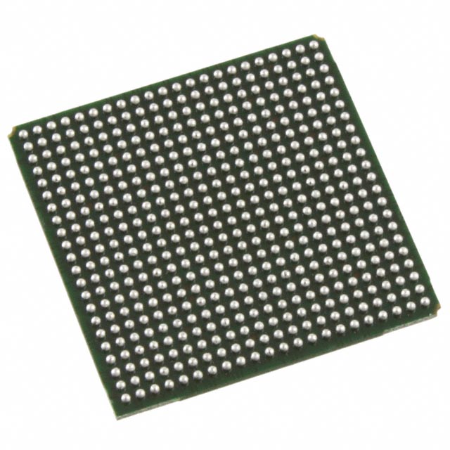
The LFXP2-17E-5FN484C is an enhanced 17k LUT (Look-Up Table) FPGA with a 5.0V I/O voltage and a 484-pin fine-pitch ball grid array (FBGA) package. It is designed to provide high-density logic integration, low power consumption, and a small footprint, making it suitable for various applications in industries such as communications, industrial, medical, and consumer electronics.
Features:
- 17,000 LUTs: The LFXP2-17E-5FN484C offers a high-density logic integration, allowing for complex designs and functionality.
- 5.0V I/O Voltage: This device is designed to support a 5.0V I/O voltage, making it compatible with a wide range of external components and systems.
- 484-pin Fine-Pitch Ball Grid Array (FBGA) Package: The compact FBGA package provides a small form factor and high-density I/O, making it suitable for space-constrained applications.
- Low Power Consumption: The LFXP2-17E-5FN484C is designed for low power operation, making it an ideal choice for battery-powered or energy-sensitive applications.
- Versatile I/O Options: The device offers a range of I/O options, including LVDS, DDR, and high-speed transceivers, providing flexibility for various interface requirements.
- In-System Programmability (ISP): The LFXP2-17E-5FN484C supports in-system programming, allowing for easy updates and reconfiguration during the development process.
Applications:
- Communications: The LFXP2-17E-5FN484C can be used in various communication systems, such as transceivers, line cards, and network infrastructure equipment.
- Industrial: This FPGA is suitable for industrial applications like motor control, machine vision, and process automation systems.
- Medical: The LFXP2-17E-5FN484C can be used in medical imaging, patient monitoring, and diagnostic equipment.
- Consumer Electronics: The device can be employed in consumer electronics such as set-top boxes, gaming consoles, and home automation systems.
- Automotive: The LFXP2-17E-5FN484C can be utilized in automotive applications like infotainment systems, advanced driver assistance systems (ADAS), and in-vehicle networking.
In summary, Lattice Semiconductor's LFXP2-17E-5FN484C is a versatile, low-power FPGA with a compact form factor, making it suitable for a wide range of applications across various industries. Its high-density logic integration, flexible I/O options, and in-system programmability make it an attractive choice for designers looking to implement complex and power-efficient solutions.
Tech Specifications
LFXP2-17E-5FN484C Documents
Download datasheets and manufacturer documentation for LFXP2-17E-5FN484C
Alternate Assembly/Test Site 14/Apr/2014 XP2 Family Product Selector Guide All Dev Pkg Mark Chg 12/Nov/2018 XP2 Family Multiple Devices Cu Wire 01/Jul/2013 Top Mark Format Change 20/Dec/2023 Related Parts


Relevant Search
Shopping Guide


.png?x-oss-process=image/format,webp/resize,h_32)


©2025 ERSA Electronics Corporation.