
 German
 Japanese
 Portuguese
 Korea
Korea
 Mexico
 Dutch
Dutch


Lattice Semiconductor
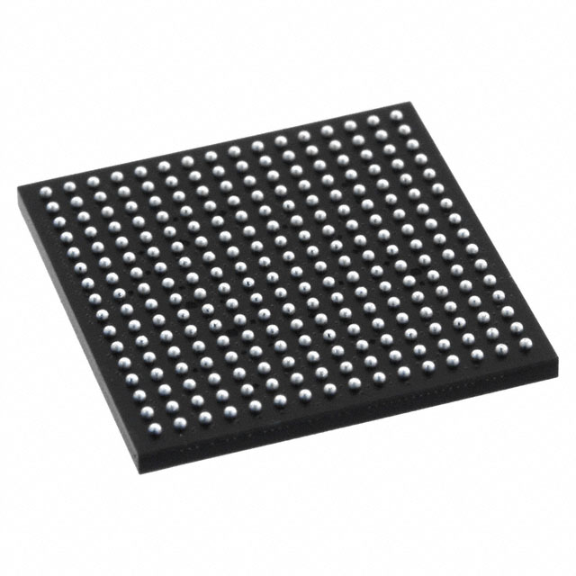
LFXP2-30E-5FTN256C

Why Choose Us?
Professional Platform
B2B & B2C purchasingDelivery at full speed
1-2 days deliveryWide variety
Original manufacturers365 days guarantee
Responsible quality
.png)


Tech Specifications
LFXP2-30E-5FTN256C Description
Lattice Semiconductor's LFXP2-30E-5FTN256C is a high-performance FPGA (Field-Programmable Gate Array) device that offers a range of features and applications for various industries.
Description:
The LFXP2-30E-5FTN256C is a member of Lattice Semiconductor's XP2 family of FPGAs. It is a mid-range device that provides a balance of performance, power, and cost. The device is available in a 256-ball fine-pitch ball grid array (FBGA) package, making it suitable for a wide range of applications.
Features:
- Performance: The LFXP2-30E-5FTN256C offers high performance with its 1.2 GHz transceiver and 1300 MHz FPGA core, making it suitable for demanding applications.
- Low Power: The device is designed for low power consumption, with a typical power consumption of 1.95 Watts.
- Security: The LFXP2-30E-5FTN256C includes advanced security features, such as secure boot, encrypted bitstream storage, and user-defined security partitions.
- Integration: The device offers a high level of integration, with a range of I/O options, including LVDS, DDR, and Gigabit Ethernet.
- Flexibility: The FPGA is highly customizable, allowing users to tailor the device to their specific needs.
Applications:
The LFXP2-30E-5FTN256C is suitable for a wide range of applications, including:
- Communications: The device's high-speed transceivers and low power consumption make it ideal for communication applications, such as 5G infrastructure and optical networking.
- Industrial Automation: The FPGA's flexibility and security features make it well-suited for industrial automation applications, such as motor control and machine vision.
- Automotive: The LFXP2-30E-5FTN256C can be used in automotive applications, such as advanced driver assistance systems (ADAS) and in-vehicle infotainment systems.
- Consumer Electronics: The device's low power consumption and high performance make it suitable for consumer electronics, such as smart home devices and wearable technology.
- Aerospace and Defense: The FPGA's security features and reliability make it suitable for aerospace and defense applications, such as satellite communication systems and radar processing.
In summary, Lattice Semiconductor's LFXP2-30E-5FTN256C is a versatile FPGA device that offers high performance, low power consumption, and advanced security features. Its wide range of applications makes it an excellent choice for industries such as communications, industrial automation, automotive, consumer electronics, and aerospace and defense.
FAQ
Not available to buy online? Want the lower wholesale price? Please Send RFQ to get best price, we will respond immediately


.png?x-oss-process=image/format,webp/resize,h_32)


