
 German
 Japanese
 Portuguese
 Korea
Korea
 Mexico
 Dutch
Dutch


Lattice Semiconductor
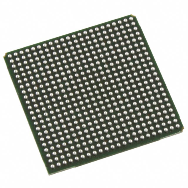
LFXP2-40E-7FN484C

Why Choose Us?
Professional Platform
B2B & B2C purchasingDelivery at full speed
1-2 days deliveryWide variety
Original manufacturers365 days guarantee
Responsible quality
.png)


Tech Specifications
LFXP2-40E-7FN484C Description
Lattice Semiconductor's LFXP2-40E-7FN484C is a high-performance programmable logic device that offers a range of features and applications for various industries.
Description:
The LFXP2-40E-7FN484C is a field programmable gate array (FPGA) that is designed to provide high performance, low power consumption, and flexible programmability. It is based on Lattice Semiconductor's low-power FPGA technology and is available in a 7x8 mm fine-pitch ball grid array (FBGA) package.
Features:
- High-performance programmable logic: The LFXP2-40E-7FN484C offers a high-density programmable logic fabric that can be configured to implement a wide range of digital logic functions.
- Low power consumption: The device is designed to operate at low power levels, making it suitable for battery-powered and energy-sensitive applications.
- Flexible programmability: The LFXP2-40E-7FN484C can be programmed using Lattice Semiconductor's proprietary software tools, allowing for easy customization and reconfiguration.
- Robust I/O capabilities: The device features a wide range of input/output options, including support for LVDS, DDR, and other high-speed interfaces.
- Security features: The LFXP2-40E-7FN484C includes advanced security features, such as encryption and authentication, to protect against unauthorized access and tampering.
Applications:
The LFXP2-40E-7FN484C is suitable for a wide range of applications, including:
- Industrial control systems: The device's high performance and low power consumption make it ideal for use in industrial control systems, where reliability and energy efficiency are critical.
- Communications infrastructure: The robust I/O capabilities and support for high-speed interfaces make the LFXP2-40E-7FN484C well-suited for use in communications infrastructure, such as routers and switches.
- Automotive systems: The device's flexibility and security features make it suitable for use in automotive systems, such as infotainment systems and advanced driver assistance systems (ADAS).
- Consumer electronics: The LFXP2-40E-7FN484C can be used in a variety of consumer electronics applications, including smart home devices, wearables, and portable electronics.
- Aerospace and defense: The device's high performance and security features make it suitable for use in aerospace and defense applications, such as satellite communications and military electronics.
Overall, the LFXP2-40E-7FN484C from Lattice Semiconductor is a versatile and powerful FPGA that offers a range of features and applications for various industries. Its high performance, low power consumption, and flexible programmability make it an ideal choice for a wide range of applications.
FAQ
Not available to buy online? Want the lower wholesale price? Please Send RFQ to get best price, we will respond immediately


.png?x-oss-process=image/format,webp/resize,h_32)


