
 German
 Japanese
 Portuguese
 Korea
Korea
 Mexico
 Dutch
Dutch


Lattice Semiconductor
LFXP2-8E-5FTN256C
696-LFXP2-8E-5FTN256C

PDF Datasheet
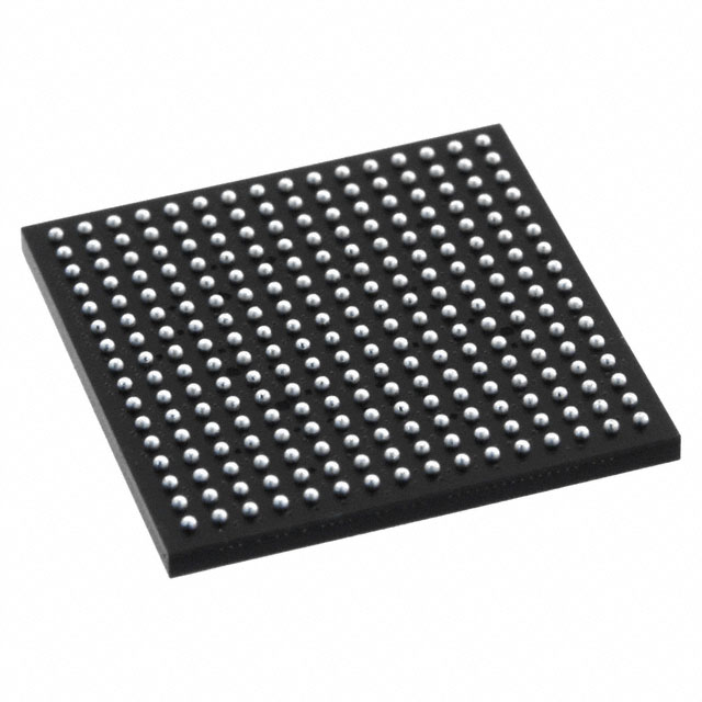
FPGA 8K Cells, 201 I/O, 1.2V, LBGA, 17x17mm
20 Weeks
Why Choose Us?
Professional Platform
B2B & B2C purchasingDelivery at full speed
1-2 days deliveryWide variety
Original manufacturers365 days guarantee
Responsible quality
.png)


Tech Specifications
Package/Case
LBGA
Density
239Kb
Height
1.25mm
Lead Free
Lead Free
Length
17mm
Max Operating Temperature
85°C
Min Operating Temperature
0°C
Max Supply Voltage
1.26V
LFXP2-8E-5FTN256C Description
XP2 Field Programmable Gate Array (FPGA) IC 201 226304 8000 256-LBGA
FAQ
What is LFXP2-8E-5FTN256C?
LFXP2-8E-5FTN256C is a FPGAs from Lattice Semiconductor. This product page provides its main specifications, pricing information, availability, and inquiry options.
What voltage specification is listed for LFXP2-8E-5FTN256C?
Is LFXP2-8E-5FTN256C currently in stock?
Are there related or alternative parts for LFXP2-8E-5FTN256C?
What operating temperature range does LFXP2-8E-5FTN256C support?
Quick Quote
ADD TO RFQ LIST
Not available to buy online? Want the lower wholesale price? Please Send RFQ to get best price, we will respond immediately
QUICK RFQ


.png?x-oss-process=image/format,webp/resize,h_32)


