
 German
 Japanese
 Portuguese
 Korea
Korea
 Mexico
 Dutch
Dutch


Microchip Technology
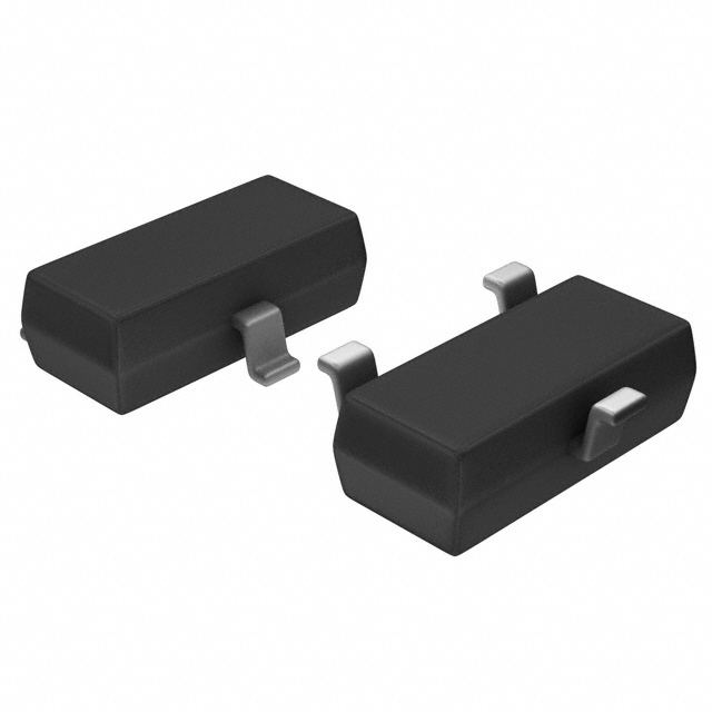
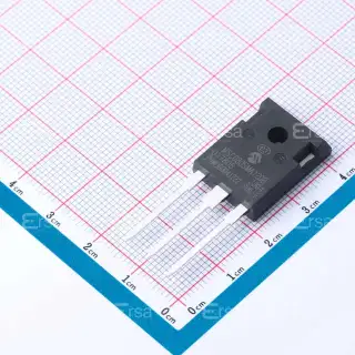
TP5335K1-G

Why Choose Us?
Professional Platform
B2B & B2C purchasingDelivery at full speed
1-2 days deliveryWide variety
Original manufacturers365 days guarantee
Responsible quality
.png)


Tech Specifications
TP5335K1-G Description
TP5335K1-G Description
The TP5335K1-G is a high-performance MOSFET (Metal Oxide) device manufactured by Microchip Technology. This P-channel device is designed for applications requiring robust power dissipation and high drain-source voltage ratings. With a maximum power dissipation of 360mW and a drain-to-source voltage of 350V, the TP5335K1-G is well-suited for various electronic systems.
TP5335K1-G Features
- Input Capacitance (Ciss): The TP5335K1-G boasts a maximum input capacitance of 110 pF at 25V, ensuring fast switching and minimal signal distortion.
- Drain to Source Voltage (Vdss): Capable of withstanding up to 350V, this MOSFET is ideal for high-voltage applications.
- Power Dissipation (Max): The device can handle a maximum power dissipation of 360mW, making it suitable for demanding power management tasks.
- Technology: Utilizing advanced MOSFET technology, the TP5335K1-G offers improved performance and reliability.
- Mounting Type: Surface mount design for easy integration into modern electronic systems.
- Rds On (Max) @ Id, Vgs: With a maximum on-resistance of 30Ohm at 200mA and 10V, the TP5335K1-G provides efficient current flow and reduced power loss.
TP5335K1-G Applications
The TP5335K1-G is an excellent choice for various applications, including:
- Power Management: Due to its high power dissipation and drain-source voltage ratings, this MOSFET is ideal for power management systems in consumer electronics.
- Automotive Electronics: The robust design and high voltage make it suitable for automotive electronics, such as ignition systems and powertrain controls.
- Industrial Control Systems: The TP5335K1-G's performance benefits are well-suited for industrial control systems, where reliability and efficiency are critical.
Conclusion of TP5335K1-G
The TP5335K1-G from Microchip Technology stands out as a reliable and high-performing MOSFET, offering unique advantages such as high input capacitance, power dissipation, and drain-source voltage ratings. Its surface mount design and advanced MOSFET technology make it an ideal choice for a wide range of applications, from power management to automotive electronics. With its compliance with REACH and RoHS3 standards, the TP5335K1-G is not only a high-performance solution but also an environmentally responsible choice for electronic design engineers.
FAQ
Not available to buy online? Want the lower wholesale price? Please Send RFQ to get best price, we will respond immediately


.png?x-oss-process=image/format,webp/resize,h_32)


