


Nexperia
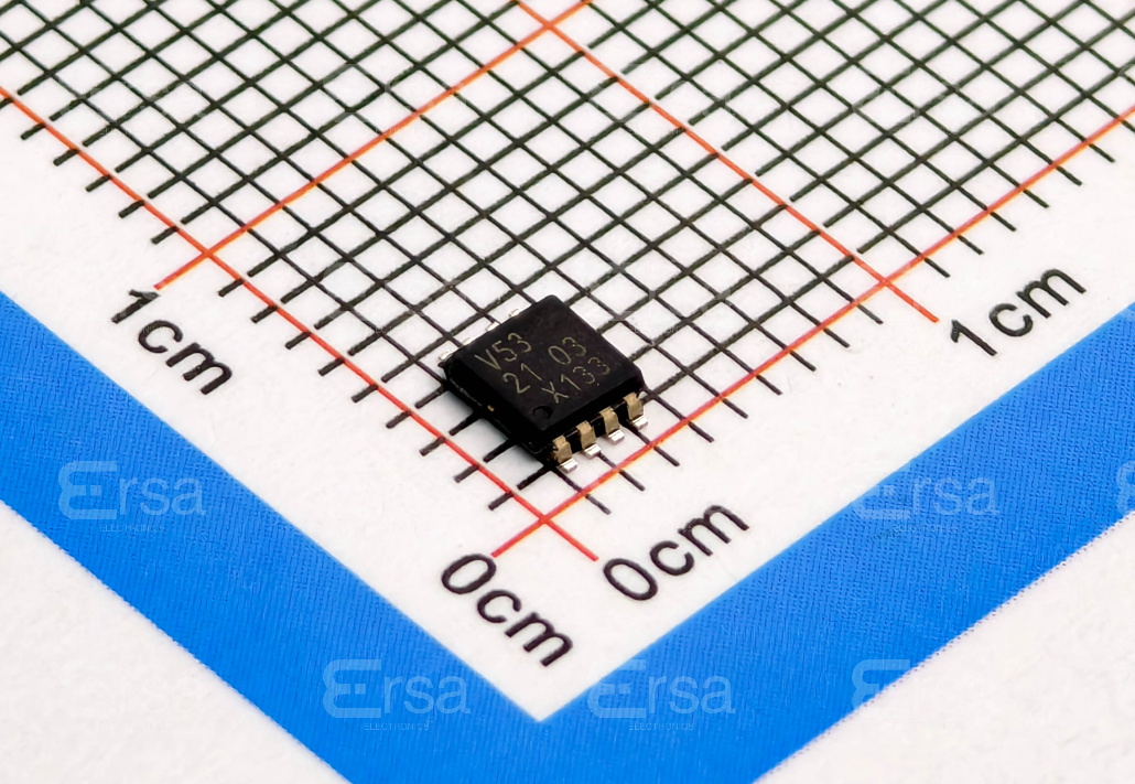
74LVC1G53DP,125
Analog Switches, Multiplexers, Demultiplexers

Not available to buy online? Want the lower wholesale price? Please Send RFQ to get best price, we will respond immediately


- 1+
- $0.34445
- $0.34
- 10+
- $0.27324
- $2.73
- 30+
- $0.24343
- $7.3
- 100+
- $0.20700
- $20.7
- 500+
- $0.16891
- $84.45
- 1000+
- $0.15898
- $158.98

.png?x-oss-process=image/format,webp/resize,p_30)


74LVC1G53DP,125 Description
74LVC1G53DP,125 Description
The 74LVC1G53DP,125 is a high-performance, single-pole double-throw (SPDT) analog switch from Nexperia, designed for applications requiring low on-state resistance and high bandwidth. This device is part of the 74LVC series and is available in an 8-pin TSSOP package. With a maximum on-state resistance of 10 ohms and a -3dB bandwidth of 300 MHz, the 74LVC1G53DP,125 offers excellent performance in a wide range of applications.
74LVC1G53DP,125 Features
- Low On-State Resistance: The 74LVC1G53DP,125 has a maximum on-state resistance of 10 ohms, ensuring minimal signal loss and distortion in high-speed applications.
- High Bandwidth: With a -3dB bandwidth of 300 MHz, this switch is ideal for high-speed signal routing and multiplexing applications.
- Low Charge Injection: The 74LVC1G53DP,125 has a charge injection of 7.5 pC, minimizing the impact on signal integrity in precision applications.
- Fast Switching Times: The maximum switch times for both ton and toff are 3.8 ns, enabling rapid signal routing and multiplexing.
- Low Leakage Current: The maximum leakage current (IS(off)) is 5 µA, ensuring low power consumption in standby modes.
- Low Channel Capacitance: The channel capacitance (CS(off), CD(off)) is 6 pF, minimizing signal distortion and ensuring high-speed performance.
- RoHS Compliant: The 74LVC1G53DP,125 is compliant with RoHS3 regulations, making it suitable for environmentally friendly applications.
- REACH Unaffected: This device is not affected by the REACH regulation, ensuring ongoing availability and compliance with European chemical regulations.
74LVC1G53DP,125 Applications
The 74LVC1G53DP,125 is ideal for a wide range of applications, including:
- Audio and Video Signal Routing: The low on-state resistance and high bandwidth make this switch suitable for routing audio and video signals in professional audio equipment and video processing systems.
- Automotive Sensor Interfaces: The 74LVC1G53DP,125 can be used to interface various sensors in automotive applications, such as engine control units, where high-speed signal routing and low power consumption are critical.
- Industrial Control Systems: In industrial control systems, this switch can be used for signal multiplexing and routing, ensuring reliable and high-speed signal transmission.
- Medical Equipment: The low leakage current and low channel capacitance make the 74LVC1G53DP,125 suitable for use in medical equipment, where signal integrity and low power consumption are essential.
Conclusion of 74LVC1G53DP,125
The 74LVC1G53DP,125 from Nexperia is a versatile and high-performance SPDT analog switch, offering low on-state resistance, high bandwidth, and fast switching times. Its low leakage current, low channel capacitance, and RoHS compliance make it an ideal choice for a wide range of applications, including audio and video signal routing, automotive sensor interfaces, industrial control systems, and medical equipment. With its unique combination of performance, reliability, and environmental compliance, the 74LVC1G53DP,125 is a valuable addition to any high-speed signal routing and multiplexing solution.
Tech Specifications
74LVC1G53DP,125 Documents
Download datasheets and manufacturer documentation for 74LVC1G53DP,125
Mult Dev Assembly Site Add 31/Dec/2018 74LVC1G53GS115 Datasheet All Dev Label Chgs 2/Aug/2020 Label Chg 12/Mar/2017 74LVC1G53GS115 Datasheet Related Parts


Shopping Guide


.png?x-oss-process=image/format,webp/resize,h_32)


©2025 ERSA Electronics Corporation.