

NXP Semiconductors
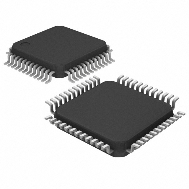
LPC1113FBD48/302,1
Microcontrollers

Not available to buy online? Want the lower wholesale price? Please Send RFQ to get best price, we will respond immediately


.png?x-oss-process=image/format,webp/resize,p_30)


LPC1113FBD48/302,1 Description
The LPC1113FBD48/302,1 is a low-power, high-performance microcontroller (MCU) developed by NXP Semiconductors. It belongs to the LPC100 series, which is designed for a wide range of embedded applications that require low power consumption, high performance, and a small form factor.
Description:
The LPC1113FBD48/302,1 is an entry-level MCU based on the 32-bit ARM Cortex-M0 processor. It operates at a maximum frequency of 50 MHz and features a high-performance memory architecture, including 16 kB of on-chip RAM and up to 512 kB of on-chip flash memory for program and data storage.
Features:
- ARM Cortex-M0 processor core with a maximum frequency of 50 MHz.
- 16 kB of on-chip RAM and up to 512 kB of on-chip flash memory.
- Low-power design with several power-saving modes, including Sleep, Deep Sleep, and Power-down modes.
- Flexible clocking options, including an internal RC oscillator, an external clock input, or an external low-swing clock input.
- A wide range of communication interfaces, such as I2C, SPI, and USART (UART).
- Support for USB 1.1 with a full-speed (12 Mbps) interface.
- On-chip analog-to-digital converter (ADC) with up to 10 channels.
- Programmable general-purpose input/output (GPIO) pins with various functions and configurations.
- Integrated voltage regulator and power-on reset (POR) circuit.
- Small form factor package options, including BGA and LQFP packages.
Applications:
The LPC1113FBD48/302,1 is suitable for a variety of embedded applications that require low power consumption, high performance, and a small form factor. Some potential applications include:
- Industrial control and automation systems.
- Medical devices and equipment.
- Portable and wearable electronics.
- Consumer electronics, such as smart home devices and IoT devices.
- Automotive control systems and accessories.
- Energy harvesting and power management systems.
- Wireless sensor networks and data acquisition systems.
- Human-Machine Interface (HMI) devices and control panels.
- Embedded systems in robotics and automation.
The LPC1113FBD48/302,1's low-power capabilities, flexible communication interfaces, and small form factor make it an ideal choice for a wide range of embedded applications where power efficiency and compact design are critical.
Tech Specifications
LPC1113FBD48/302,1 Documents
Download datasheets and manufacturer documentation for LPC1113FBD48/302,1
LPC1110-15 All Dev Label Update 15/Dec/2020 Mult Dev Pkg Chgs 20/Sep/2020 LPC111x/LPC11Cxx Manual LPC1110-15 Multi Design 02/25/2022 NXP USA Inc REACH NXP USA Inc RoHS Cert Related Parts


Shopping Guide


.png?x-oss-process=image/format,webp/resize,h_32)


©2025 ERSA Electronics Corporation.