NXP Semiconductors_LPC1313FBD48/01,15

NXP Semiconductors
LPC1313FBD48/01,15  
Microcontrollers

NXP Semiconductors
LPC1313FBD48/01,15
685-LPC1313FBD48/01,15
Ersa
NXP Semiconductors-LPC1313FBD48/01,15-datasheets-11945705.pdf
IC MCU 32BIT 32KB FLASH 48LQFP
In Stock : 1738

Not available to buy online? Want the lower wholesale price? Please Send RFQ to get best price, we will respond immediately

QUICK RFQ
ADD TO RFQ LIST
ersa FreeSample ersa flow
  • Quantity
  • Unit Price
  • Ext. Price
    • 1+
    • $6.43025
    • $6.43
    • 10+
    • $5.59397
    • $55.94
    • 30+
    • $5.08392
    • $152.52
    ADD TO CART
    QUICK ORDER
    $6.43025    $6.43
    ISO9001
    Quality Policy
    ISO45001
    ISO14001

    LPC1313FBD48/01,15 Description

    The LPC1313FBD48/01,15 is a low-power, high-performance microcontroller unit (MCU) developed by NXP Semiconductors. It belongs to the LPC13xx family of MCUs, which are designed for a wide range of embedded applications.

    Description:

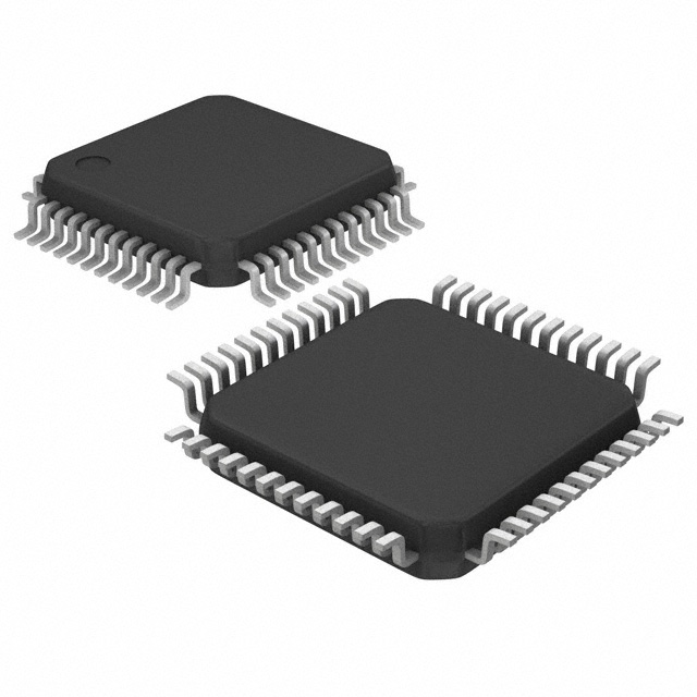
    The LPC1313FBD48/01,15 is a 48-pin QFN package MCU with an embedded ARM Cortex-M0 CPU. It operates at a core frequency of up to 50 MHz, providing high computational performance for its class. The device features 16 kB of on-chip RAM and 64 kB of on-chip flash memory, allowing for efficient data storage and program execution.

    Features:

    1. ARM Cortex-M0 CPU with a core frequency of up to 50 MHz.
    2. 48-pin QFN package.
    3. 16 kB on-chip RAM.
    4. 64 kB on-chip flash memory.
    5. Low-power consumption with various power-saving modes.
    6. Integrated peripheral set, including UART, SPI, I2C, and USB interfaces.
    7. 34 general-purpose I/O pins with multiple functions.
    8. 4-channel DMA controller for efficient data transfer.
    9. 10-bit ADC with up to 8 channels.
    10. Flexible clock management system with an internal RC oscillator or external clock sources.

    Applications:

    The LPC1313FBD48/01,15 is suitable for a wide range of embedded applications due to its low-power consumption, high performance, and versatile features. Some of the potential applications include:

    1. Industrial control and automation systems.
    2. Medical devices and equipment.
    3. Portable electronics and wearable devices.
    4. Home automation and IoT devices.
    5. Consumer electronics, such as smart appliances and multimedia devices.
    6. Automotive infotainment and body control systems.
    7. Wireless communication devices, such as Zigbee or Bluetooth modules.
    8. Data acquisition and signal processing systems.
    9. Battery-powered devices, where low power consumption is critical.

    The LPC1313FBD48/01,15 is a versatile and powerful MCU that can be used in various embedded applications requiring low power consumption and high performance. Its extensive feature set and flexible clock management system make it an ideal choice for developers looking to create energy-efficient and high-performance embedded systems.

    Tech Specifications

    Unit Weight
    Program Memory Type
    Analog Supply Voltage
    PPAP
    Data Bus Width (bit)
    Product Status
    SPI
    Automotive
    RoHS
    EEPROM Size
    Supplier Package
    Package / Case
    Processor Series
    Instruction Set Architecture
    Core Architecture
    REACH Status
    Maximum Clock Frequency
    Family Name
    Maximum Operating Supply Voltage (V)
    Maximum Clock Rate (MHz)
    EU RoHS
    Data RAM Size
    Moisture Sensitivity Level (MSL)
    Core
    Operating Temperature
    ECCN
    Mounting Type
    Standard Package Name
    Oscillator Type
    Pin Count
    Mounting
    Parallel Master Port
    CAN
    USART
    Core Size
    Ethernet
    Connectivity
    SVHC
    Program Memory Size
    Typical Operating Supply Voltage (V)
    HTSUS
    Package
    Data Converters
    USHTS
    Programmability
    Core Processor
    PCB changed
    HTS
    I/O Voltage
    ECCN (US)
    Real Time Clock
    ADC Resolution
    Maximum Power Dissipation (mW)
    Device Core
    Supplier Device Package
    Supply Voltage - Min
    ADC Channels
    Minimum Operating Temperature (°C)
    Maximum Operating Temperature (°C)
    No. of Timers
    Package Height
    Data RAM Type
    Mfr
    Maximum Operating Temperature
    I2C
    Supply Voltage - Max
    Voltage - Supply (Vcc/Vdd)
    Interface Type
    RoHS Status
    Maximum CPU Frequency (MHz)
    Mounting Style
    Speed
    Number of ADCs
    Data Bus Width
    USB
    RAM Size
    Number of I/O
    UART
    Peripherals
    I2S
    Package Length
    ADC Resolution (bit)
    Minimum Operating Temperature
    Number of Timers/Counters
    Series
    Watchdog
    Part Status
    Number of I/Os
    Package Width
    Number of ADC Channels
    Base Product Number
    Minimum Operating Supply Voltage (V)
    Status
    PWM [Number, bits]
    ADC [Number, bits]
    Operating Frequency [Max] (MHz)
    Serial Communication
    Core Type
    GPIO
    Supply Voltage [Min to Max] (V)
    Timers [Number, bits]
    Safe Assure Functional Safety
    PbFree
    Halogen Free
    RHF Indicator
    Ambient Operating Temperature (Min to Max) (℃)
    Flash (kB)
    SRAM (kB)

    LPC1313FBD48/01,15 Documents

    Download datasheets and manufacturer documentation for LPC1313FBD48/01,15

    Ersa LPC1311/13/42/43      
    Ersa All Dev Label Update 15/Dec/2020      
    Ersa Multi Design 02/25/2022      
    Ersa NXP USA Inc REACH       NXP USA Inc RoHS Cert      

    Shopping Guide

    Payment Methods
    Payment Methods include Prepayment TT (bank transfer), Western Union, and PayPal. Customers are responsible for shipping costs, bank charges, customs duties and taxes.
    Shipping Rate
    Shipments are made once a day around 5pm, excluding Sundays. Once shipped, the estimated delivery time is usually 5-7 business days, depending on the courier you choose.
    Delivery Methods
    Provide DHL, FedEx, UPS, EMS, SF Express and Registered Airmail International Delivery Service