
 German
 Japanese
 Portuguese
 Korea
Korea
 Mexico
 Dutch
Dutch


NXP Semiconductors
LPC1313FBD48,151

Why Choose Us?
Professional Platform
B2B & B2C purchasingDelivery at full speed
1-2 days deliveryWide variety
Original manufacturers365 days guarantee
Responsible quality
.png)


Tech Specifications
LPC1313FBD48,151 Description
The LPC1313FBD48,151 is a microcontroller unit (MCU) manufactured by NXP Semiconductors. This MCU belongs to the LPC1300 series, which is known for its low power consumption, high performance, and a range of integrated features.
Description:
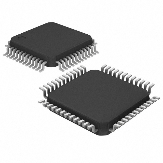
The LPC1313FBD48,151 is a 32-bit ARM Cortex-M0 based MCU. It is housed in a 48-pin LQFP (Low Profile Quad Flat Package) package. The device is designed for a wide range of embedded applications that require low power consumption and high performance.
Features:
-
ARM Cortex-M0 Processor: The LPC1313FBD48,151 features an ARM Cortex-M0 processor with a clock speed of up to 50 MHz, providing high performance for a wide range of applications.
-
Memory: The device comes with 16 kB of on-chip RAM and 64 kB of on-chip flash memory for program storage.
-
I/O Interfaces: The LPC1313FBD48,151 offers a variety of I/O interfaces, including UART, SPI, I2C, and USB, making it suitable for communication with various peripherals.
-
GPIO: The device has 21 GPIO (General-Purpose Input/Output) pins, which can be configured for different functions, such as digital input/output, analog input, or as alternate function pins for the I/O interfaces.
-
Power Management: The LPC1313FBD48,151 features a range of power-saving modes, including sleep, deep sleep, and power-down modes, to minimize power consumption in low-power applications.
-
Analog-to-Digital Converter (ADC): The MCU includes a 10-bit ADC with up to 8 channels, allowing for the conversion of analog signals to digital values.
-
Programmable Delay Block: The device features a programmable delay block, which can be used for generating precise time delays in various applications.
Applications:
The LPC1313FBD48,151 is suitable for a wide range of embedded applications, including but not limited to:
-
Industrial Control: The device can be used in industrial control systems for monitoring and controlling various parameters.
-
Medical Devices: The low power consumption and high performance make it suitable for battery-powered medical devices, such as portable monitoring equipment.
-
Consumer Electronics: The LPC1313FBD48,151 can be used in consumer electronics, such as home automation systems, smart appliances, and portable devices.
-
Automotive Applications: The MCU can be employed in automotive applications, such as infotainment systems, body control modules, and engine control units.
-
IoT Devices: The integrated USB and wireless communication interfaces make the LPC1313FBD48,151 suitable for Internet of Things (IoT) devices, such as smart sensors and wearable devices.
-
Data Acquisition Systems: The ADC and programmable delay block features make the device suitable for data acquisition systems in various industries.
In summary, the LPC1313FBD48,151 is a versatile, low-power, and high-performance MCU from NXP Semiconductors that can be used in a wide range of embedded applications, from industrial control to consumer electronics and IoT devices.
FAQ
Not available to buy online? Want the lower wholesale price? Please Send RFQ to get best price, we will respond immediately


.png?x-oss-process=image/format,webp/resize,h_32)


