
 German
 Japanese
 Portuguese
 Korea
Korea
 Mexico
 Dutch
Dutch


onsemi
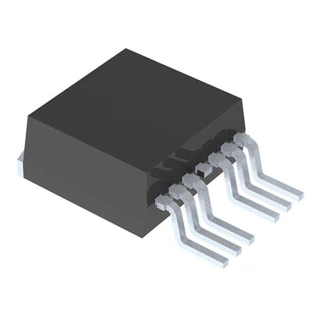
FDB047N10

Why Choose Us?
Professional Platform
B2B & B2C purchasingDelivery at full speed
1-2 days deliveryWide variety
Original manufacturers365 days guarantee
Responsible quality
.png)


Tech Specifications
FDB047N10 Description
The FDB047N10 is a high voltage N-channel MOSFET manufactured by ON Semiconductor. It is designed for use in a variety of power electronic applications, including motor control, power supplies, and energy management systems.
Description:
The FDB047N10 is an N-channel enhancement mode field effect transistor (MOSFET) with a drain-to-source voltage (VDS) of up to 100V, a continuous drain current (ID) of up to 4.7A, and a gate-source voltage (VGS) of up to 10V. It features a low on-state resistance (RDS(on)) of 4.2 mΩ max, which helps to minimize power dissipation and improve efficiency.
Features:
- N-channel, enhancement mode MOSFET
- VDS of up to 100V
- ID of up to 4.7A
- VGS of up to 10V
- Low on-state resistance (RDS(on)) of 4.2 mΩ max
- Suitable for use in a wide range of power electronic applications
Applications:
The FDB047N10 is well-suited for use in a variety of power electronic applications, including:
- Motor control
- Power supplies
- Energy management systems
- Battery management systems
- DC-DC converters
- Inverters
- Switch mode power supplies (SMPS)
- Class D audio amplifiers
Overall, the FDB047N10 is a high-performance MOSFET that offers excellent electrical characteristics and reliability, making it a popular choice for use in a wide range of power electronic applications.
FAQ
Not available to buy online? Want the lower wholesale price? Please Send RFQ to get best price, we will respond immediately


.png?x-oss-process=image/format,webp/resize,h_32)


