

onsemi
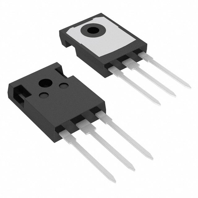
FDH055N15A
Single FETs, MOSFETs

Not available to buy online? Want the lower wholesale price? Please Send RFQ to get best price, we will respond immediately


- 1+
- $4.01911
- $4.02
- 10+
- $3.51900
- $35.19
- 30+
- $2.88144
- $86.44
- 90+
- $2.58005
- $232.2

.png?x-oss-process=image/format,webp/resize,p_30)


FDH055N15A Description
FDH055N15A is a high voltage N-channel MOSFET transistor manufactured by ON Semiconductor. Here is a brief description of the device along with its features and applications:
Description:
The FDH055N15A is an N-channel enhancement mode field effect transistor (MOSFET) designed for high voltage applications. It is a 5th generation TrenchFET technology that offers improved performance and reliability compared to previous generations.
Features:
- High Voltage: The FDH055N15A is rated for a maximum drain-source voltage (VDS) of 1500V, making it suitable for high voltage applications.
- Low On-Resistance: The device has a low on-state resistance (RDS(on)) of 0.55 ohms (typical) at a gate-source voltage (VGS) of 10V, which helps reduce power dissipation and improve efficiency.
- High Input Impedance: The MOSFET has a high input impedance, which allows it to be easily driven by a variety of control circuits.
- Avalanche Energy Rated: The FDH055N15A is designed to withstand high energy transients, making it suitable for applications where the device may be subjected to high energy pulses.
- TrenchFET Technology: The device uses 5th generation TrenchFET technology, which provides improved performance and reliability compared to previous generations.
Applications:
The FDH055N15A is suitable for a wide range of high voltage applications, including:
- Motor Control: The MOSFET can be used in motor control circuits for industrial and automotive applications.
- Power Supplies: The device can be used in high voltage power supply circuits, such as switch mode power supplies (SMPS) and uninterruptible power supplies (UPS).
- Renewable Energy: The FDH055N15A can be used in power electronics for renewable energy applications, such as solar panel inverters and wind turbine converters.
- Battery Management: The MOSFET can be used in battery management systems for electric vehicles and energy storage systems.
- Industrial Automation: The device can be used in various industrial automation applications, such as robotic control and programmable logic controllers (PLCs).
Overall, the FDH055N15A is a high performance MOSFET that offers excellent electrical characteristics and reliability for a wide range of high voltage applications.
Tech Specifications
FDH055N15A Documents
Download datasheets and manufacturer documentation for FDH055N15A
HUF7565x/FDH055x 20/Jun/2022 FDH055N15A Mult Devices 24/Oct/2017 Packing quantity increase 28/Dec/2020 Logo 17/Aug/2017 Dimension/Color Change 24/Feb/2021 onsemi RoHS onsemi REACH Material Declaration FDH055N15A Related Parts


Shopping Guide


.png?x-oss-process=image/format,webp/resize,h_32)


©2025 ERSA Electronics Corporation.