onsemi_FDS6675BZ

onsemi
FDS6675BZ  
Single FETs, MOSFETs

onsemi
FDS6675BZ
278-FDS6675BZ
Ersa
onsemi-FDS6675BZ-datasheets-6780441.pdf
MOSFET P-CH 30V 11A 8SOIC
In Stock : 127148

Not available to buy online? Want the lower wholesale price? Please Send RFQ to get best price, we will respond immediately

QUICK RFQ
ADD TO RFQ LIST
ersa FreeSample ersa flow
  • Quantity
  • Unit Price
  • Ext. Price
    • 1+
    • $0.62100
    • $0.62
    • 10+
    • $0.51336
    • $5.13
    • 30+
    • $0.45871
    • $13.76
    • 100+
    • $0.40572
    • $40.57
    ADD TO CART
    QUICK ORDER
    $0.62100    $0.62
    ISO9001
    Quality Policy
    ISO45001
    ISO14001

    FDS6675BZ Description

    The FDS6675BZ is a high-performance, integrated MOSFET driver from ON Semiconductor. It is designed to drive N-channel MOSFETs in a wide range of applications, including motor control, power management, and automotive systems.

    Description:

    The FDS6675BZ is a monolithic high-voltage MOSFET driver that provides high-speed switching and precise control of N-channel MOSFETs. It features a high-voltage input protection, a low-voltage output stage, and a high-voltage boot-strap circuit. The device is available in a small, thermally-enhanced SOIC-8 package.

    Features:

    • High-voltage input protection
    • Low-voltage output stage
    • High-voltage boot-strap circuit
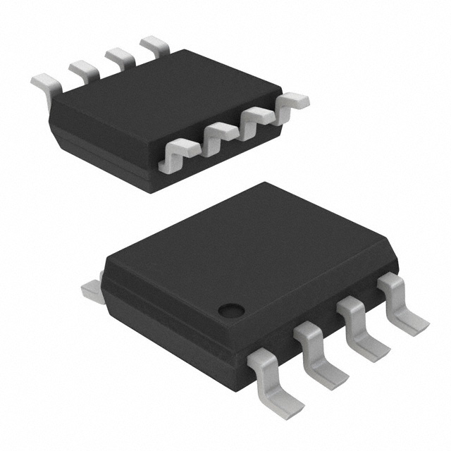
    • Small, thermally-enhanced SOIC-8 package
    • Wide operating voltage range
    • High output current capability
    • Short-circuit protection
    • Thermal shutdown protection
    • Enable input for easy control

    Applications:

    • Motor control
    • Power management
    • Automotive systems
    • Industrial control
    • Robotics
    • Battery management systems
    • Switch mode power supplies (SMPS)
    • Class D audio amplifiers

    The FDS6675BZ is a versatile MOSFET driver that can be used in a wide range of applications where high-speed switching and precise control of N-channel MOSFETs are required. Its high-voltage input protection, low-voltage output stage, and high-voltage boot-strap circuit make it suitable for use in high-voltage applications. Additionally, its short-circuit protection, thermal shutdown protection, and enable input provide added safety and flexibility for system designers.

    Tech Specifications

    FET Type
    Input Capacitance (Ciss) (Max) @ Vds
    Gate Charge (Qg) (Max) @ Vgs
    Product Status
    Supplier Device Package
    Drain to Source Voltage (Vdss)
    Power Dissipation (Max)
    Package / Case
    Technology
    REACH Status
    Mfr
    Vgs (Max)
    RoHS Status
    Moisture Sensitivity Level (MSL)
    Operating Temperature
    FET Feature
    ECCN
    Mounting Type
    Rds On (Max) @ Id, Vgs
    Vgs(th) (Max) @ Id
    Series
    Current - Continuous Drain (Id) @ 25°C
    Drive Voltage (Max Rds On, Min Rds On)
    HTSUS
    Package
    Base Product Number
    Configuration
    Typical Turn-Off Delay Time (ns)
    Maximum Gate Source Leakage Current (nA)
    Typical Rise Time (ns)
    PPAP
    Channel Mode
    Typical Turn-On Delay Time (ns)
    Automotive
    Supplier Package
    Maximum IDSS (uA)
    Channel Type
    EU RoHS
    Maximum Continuous Drain Current (A)
    Maximum Pulsed Drain Current @ TC=25°C (A)
    Maximum Drain Source Voltage (V)
    Maximum Drain Source Resistance (mOhm)
    Standard Package Name
    Maximum Continuous Drain Current on PCB @ TC=25°C (A)
    Pin Count
    Mounting
    Minimum Gate Threshold Voltage (V)
    Typical Reverse Transfer Capacitance @ Vds (pF)
    Lead Shape
    Typical Gate to Drain Charge (nC)
    Typical Gate Charge @ Vgs (nC)
    Typical Input Capacitance @ Vds (pF)
    Maximum Power Dissipation on PCB @ TC=25°C (W)
    Category
    PCB changed
    HTS
    Number of Elements per Chip
    ECCN (US)
    Maximum Power Dissipation (mW)
    Minimum Operating Temperature (°C)
    Maximum Operating Temperature (°C)
    Typical Fall Time (ns)
    Process Technology
    Package Height
    Typical Gate to Source Charge (nC)
    Maximum Positive Gate Source Voltage (V)
    Typical Gate Threshold Voltage (V)
    Maximum Gate Source Voltage (V)
    Typical Gate Plateau Voltage (V)
    Package Length
    Typical Gate Charge @ 10V (nC)
    Maximum Diode Forward Voltage (V)
    Typical Diode Forward Voltage (V)
    Operating Junction Temperature (°C)
    Typical Output Capacitance (pF)
    Part Status
    Maximum Gate Threshold Voltage (V)
    Package Width
    Maximum Junction Ambient Thermal Resistance on PCB (°C/W)

    FDS6675BZ Documents

    Download datasheets and manufacturer documentation for FDS6675BZ

    Ersa Wafer 6/8 Inch Addition 16/Jun/2014      
    Ersa FDS6675BZ Datasheet      
    Ersa Mult Devices 24/Oct/2017       Mult MSL1 Pkg Chg 20/Dec/2018      
    Ersa Logo 17/Aug/2017       Mold Compound 12/Dec/2007      
    Ersa onsemi RoHS       onsemi REACH       Material Declaration FDS6675BZ      

    Shopping Guide

    Payment Methods
    Payment Methods include Prepayment TT (bank transfer), Western Union, and PayPal. Customers are responsible for shipping costs, bank charges, customs duties and taxes.
    Shipping Rate
    Shipments are made once a day around 5pm, excluding Sundays. Once shipped, the estimated delivery time is usually 5-7 business days, depending on the courier you choose.
    Delivery Methods
    Provide DHL, FedEx, UPS, EMS, SF Express and Registered Airmail International Delivery Service