
 German
 Japanese
 Portuguese
 Korea
Korea
 Mexico
 Dutch
Dutch


onsemi
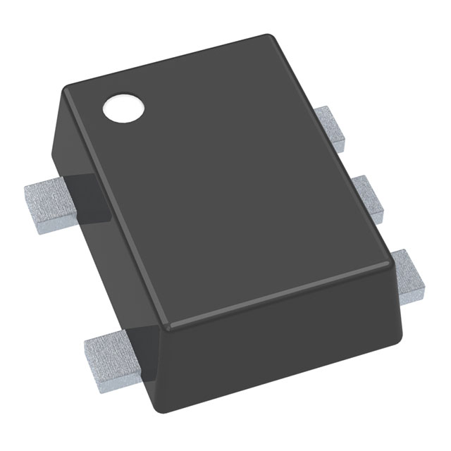
NL17SV08XV5T2G

Why Choose Us?
Professional Platform
B2B & B2C purchasingDelivery at full speed
1-2 days deliveryWide variety
Original manufacturers365 days guarantee
Responsible quality
.png)


Tech Specifications
NL17SV08XV5T2G Description
NL17SV08XV5T2G Description
The NL17SV08XV5T2G is a high-performance, 2-input AND gate from onsemi, designed for applications requiring fast signal propagation and low power consumption. This Surface Mount device features a max propagation delay of 2.3ns @ 3V, 30pF, making it ideal for high-speed digital circuits. With a supply voltage range of 0.9V to 3.6V, the NL17SV08XV5T2G offers flexibility in various power supply scenarios.
NL17SV08XV5T2G Features
- Logic Type: AND Gate
- Max Propagation Delay: 2.3ns @ 3V, 30pF
- Supply Voltage: 0.9V to 3.6V
- Input Logic Levels: Low (0.7V to 0.8V), High (1.6V to 2V)
- Number of Inputs: 2
- Number of Circuits: 1
- Current - Quiescent (Max): 900 nA
- Current - Output High, Low: 24mA, 24mA
- RoHS Compliance: ROHS3 Compliant
- REACH Status: REACH Unaffected
- Moisture Sensitivity Level (MSL): 1 (Unlimited)
NL17SV08XV5T2G Applications
The NL17SV08XV5T2G is well-suited for various applications in the electronics industry, including:
- Digital Circuits: Its fast propagation delay and low power consumption make it ideal for high-speed digital circuits.
- Signal Processing: The device's ability to handle a wide supply voltage range is beneficial in signal processing applications.
- Automotive Electronics: The NL17SV08XV5T2G's robust performance and low quiescent current make it suitable for automotive electronics, where reliability and efficiency are crucial.
- Telecommunications: In telecommunications, the device's fast signal propagation and low power consumption are essential for maintaining high-speed data transmission.
Conclusion of NL17SV08XV5T2G
The NL17SV08XV5T2G from onsemi stands out for its fast propagation delay, low power consumption, and wide supply voltage range. Its unique features, such as the ability to handle a wide range of input logic levels and its compliance with RoHS and REACH regulations, make it an excellent choice for high-speed digital circuits, signal processing, automotive electronics, and telecommunications applications. With its reliable performance and versatility, the NL17SV08XV5T2G is a valuable addition to any electronics engineer's toolbox.
FAQ
| Quantity | Unit Price | Ext. Price |
|---|---|---|
| 1+ | $0.14080 | $0.14 |
| 10+ | $0.09592 | $0.96 |
| 25+ | $0.08413 | $2.10 |
| 100+ | $0.07146 | $7.15 |
| 250+ | $0.06537 | $16.34 |
Not available to buy online? Want the lower wholesale price? Please Send RFQ to get best price, we will respond immediately


.png?x-oss-process=image/format,webp/resize,h_32)


