

onsemi
NTHD3101FT1G
Single FETs, MOSFETs

Not available to buy online? Want the lower wholesale price? Please Send RFQ to get best price, we will respond immediately


.png?x-oss-process=image/format,webp/resize,p_30)


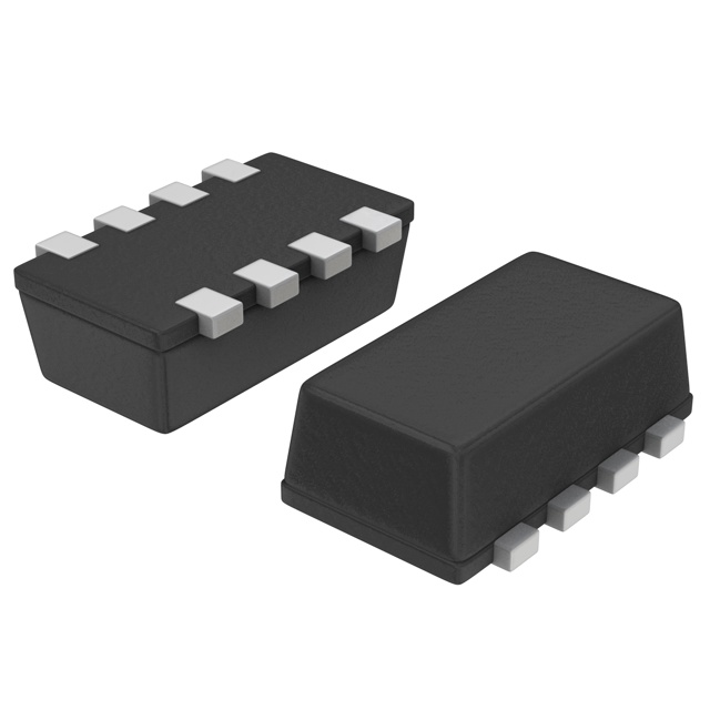
NTHD3101FT1G Description
NTHD3101FT1G Description
The NTHD3101FT1G is a high-performance MOSFET (Metal Oxide) device from onsemi, designed for a wide range of applications in the electronics industry. This Single FET is a P-Channel device with a drain-source voltage (Vdss) of 20V and a continuous drain current (Id) of 3.2A at 25°C. The device is packaged in a ChipFET™ package and is surface mount compatible, making it ideal for space-constrained applications.
NTHD3101FT1G Features
- High Input Capacitance (Ciss): With a maximum input capacitance of 680 pF at 10V, the NTHD3101FT1G offers fast switching capabilities, reducing power consumption and improving overall performance.
- Low Gate Charge (Qg): The maximum gate charge of 7.4 nC at 4.5V ensures efficient gate control and minimizes power loss during switching.
- Low Rds On: The maximum Rds On of 80 mOhm at 3.2A and 4.5V provides low on-resistance, reducing power dissipation and improving efficiency.
- Schottky Diode Feature: The integrated Schottky diode offers protection against voltage spikes and reverse current, enhancing the device's reliability and durability.
- Compliance with Industry Standards: The NTHD3101FT1G is REACH unaffected, RoHS3 compliant, and EAR99 classified, ensuring compliance with environmental and regulatory standards.
NTHD3101FT1G Applications
The NTHD3101FT1G is ideal for various applications where high performance, low power consumption, and reliability are critical. Some specific use cases include:
- Power Management: In power supply circuits, the device's low Rds On and high Vdss make it suitable for efficient power distribution and regulation.
- Motor Control: The NTHD3101FT1G's high current handling capability and fast switching speed are ideal for motor control applications, such as in industrial automation and robotics.
- Automotive Electronics: The device's ability to handle high voltages and currents, along with its robust protection features, make it suitable for automotive electronics, such as in-vehicle infotainment systems and power windows.
- Telecommunications: In telecommunications equipment, the NTHD3101FT1G can be used for signal processing and power management, benefiting from its low power consumption and fast switching capabilities.
Conclusion of NTHD3101FT1G
The NTHD3101FT1G is a versatile and high-performance MOSFET device that offers a combination of low power consumption, high efficiency, and robust protection features. Its unique combination of technical specifications and compliance with industry standards make it an ideal choice for a wide range of applications in the electronics industry. While the product is currently classified as obsolete, it remains a valuable option for applications that require its specific performance characteristics.
Tech Specifications
NTHD3101FT1G Documents
Download datasheets and manufacturer documentation for NTHD3101FT1G
NTHD3101F Obsolete Notice 15/Dec/2022 NTHD3101F onsemi RoHS Material Declaration NTHD3101FT1G Related Parts


Shopping Guide


.png?x-oss-process=image/format,webp/resize,h_32)


©2025 ERSA Electronics Corporation.