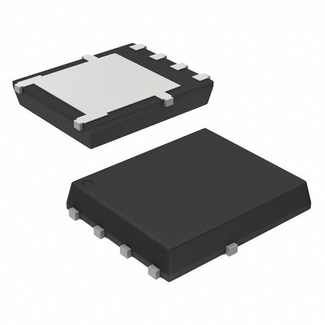
onsemi_NVMFS5113PLT1G

onsemi
NVMFS5113PLT1G  
Single FETs, MOSFETs

onsemi
NVMFS5113PLT1G
278-NVMFS5113PLT1G
Ersa
onsemi-NVMFS5113PLT1G-datasheets-5269021.pdf
MOSFET P-CH 60V 10A/64A 5DFN
In Stock : 8832

Not available to buy online? Want the lower wholesale price? Please Send RFQ to get best price, we will respond immediately

QUICK RFQ
ADD TO RFQ LIST
ersa FreeSample ersa flow
  • Quantity
  • Unit Price
  • Ext. Price
    • 1+
    • $2.35483
    • $2.35
    • 10+
    • $2.01370
    • $20.14
    • 30+
    • $1.80007
    • $54
    • 100+
    • $1.58148
    • $158.15
    • 500+
    • $1.48378
    • $741.89
    • 1500+
    • $1.44072
    • $2161.08
    ADD TO CART
    QUICK ORDER
    $2.35483    $2.35
    ISO9001
    Quality Policy
    ISO45001
    ISO14001

    NVMFS5113PLT1G Description

    The NVMFS5113PLT1G is a high-performance MOSFET from ON Semiconductor. This device is designed for use in a variety of applications, including motor control, power conversion, and industrial control systems.

    Description:

    The NVMFS5113PLT1G is a N-channel power MOSFET with a voltage rating of 100V and a continuous drain current of 75A. It features a logic level gate drive and is available in a TO-220 package.

    Features:

    • N-channel power MOSFET
    • 100V drain-to-source voltage
    • 75A continuous drain current
    • Logic level gate drive
    • TO-220 package

    Applications:

    The NVMFS5113PLT1G is suitable for a wide range of applications, including:

    1. Motor control: The device can be used in motor control applications, such as brushless DC motor control and stepper motor control.
    2. Power conversion: The MOSFET can be used in power conversion applications, such as DC-DC converters and AC-DC power supplies.
    3. Industrial control systems: The device is suitable for use in industrial control systems, such as robotic systems and conveyor systems.
    4. Automotive applications: The NVMFS5113PLT1G can be used in automotive applications, such as electric power steering and electric braking systems.

    Overall, the NVMFS5113PLT1G is a versatile MOSFET that offers high performance and reliability in a variety of applications. Its features make it an ideal choice for designers looking for a high-quality power MOSFET for their next project.

    Tech Specifications

    Unit Weight
    V gs (V)
    Configuration
    Package Name
    Input Capacitance (Ciss) (Max) @ Vds
    Gate Charge (Qg) (Max) @ Vgs
    PPAP
    OPN in older Technology
    Fall Time
    Automotive
    RoHS
    Maximum IDSS (uA)
    Typical Turn-On Delay Time
    Q gd Typ @ V GS = 4.5 V (nC)
    REACH Status
    Channel Type
    Wide SOA Mosfets
    Maximum Continuous Drain Current (A)
    MSL Temp (°C)
    Status
    Maximum Drain Source Voltage (V)
    Supplier Temperature Grade
    Rds On (Max) @ Id, Vgs
    Standard Package Name
    MSL Type
    Mounting
    C rss Typ (pF)
    Qualification
    Rise Time
    Current - Continuous Drain (Id) @ 25°C
    Vgs th - Gate-Source Threshold Voltage
    Package
    Maximum Drain Source Resistance (MOhm)
    P D Max (W)
    R DS(on) Max @ V GS = 4.5 V (mΩ)
    I D Max (A)
    C oss Typ (pF)
    Qg - Gate Charge
    Power Dissipation (Max)
    Development Kit
    Package Height
    Vgs (Max)
    Maximum Operating Temperature
    Q g Typ @ V GS = 4.5 V (nC)
    RoHS Status
    Q rr Typ (nC)
    SVHC Exceeds Threshold
    Silicon Family
    Transistor Polarity
    Typical Gate Charge @ 10V (nC)
    Minimum Operating Temperature
    Vds - Drain-Source Breakdown Voltage
    Type
    Part Status
    Maximum Gate Threshold Voltage (V)
    Package Width
    Q g Typ @ V GS = 10 V (nC)
    Typical Turn-Off Delay Time (ns)
    Maximum Gate Source Leakage Current (nA)
    Id - Continuous Drain Current
    V gs(th) Max (V)
    Typical Rise Time (ns)
    Channel Mode
    Typical Turn-On Delay Time (ns)
    Product Status
    Drain to Source Voltage (Vdss)
    Supplier Package
    Transistor Type
    Package / Case
    Number of Channels
    Technology
    EU RoHS
    Rds On - Drain-Source Resistance
    Moisture Sensitivity Level (MSL)
    Operating Temperature
    Channel Polarity
    R DS(on) Max @ V GS = 10 V (mΩ)
    ECCN
    Grade
    V (BR)DSS Min (V)
    Mounting Type
    Vgs(th) (Max) @ Id
    Pin Count
    Lead Shape
    SVHC
    Drive Voltage (Max Rds On, Min Rds On)
    HTSUS
    USHTS
    Typical Gate Charge @ Vgs (nC)
    Typical Input Capacitance @ Vds (pF)
    Category
    Case Outline
    PCB changed
    HTS
    FET Type
    Number of Elements per Chip
    ECCN (US)
    Maximum Power Dissipation (mW)
    Gate Level
    Supplier Device Package
    Minimum Operating Temperature (°C)
    C iss Typ (pF)
    Maximum Operating Temperature (°C)
    Typical Fall Time (ns)
    Mfr
    Mounting Style
    R DS(on) Max @ V GS = 2.5 V (mΩ)
    FET Feature
    Maximum Gate Source Voltage (V)
    Vgs - Gate-Source Voltage
    Typical Turn-Off Delay Time
    Package Length
    Series
    Forward Transconductance - Min
    Pd - Power Dissipation
    Base Product Number

    NVMFS5113PLT1G Documents

    Download datasheets and manufacturer documentation for NVMFS5113PLT1G

    Ersa NxMFS5113PLT1G 28/Sep/2023      
    Ersa NVMFS5113PL      
    Ersa NVMFS5113PL      
    Ersa onsemi RoHS       onsemi REACH       Material Declaration NVMFS5113PLT1G      

    Shopping Guide

    Payment Methods
    Payment Methods include Prepayment TT (bank transfer), Western Union, and PayPal. Customers are responsible for shipping costs, bank charges, customs duties and taxes.
    Shipping Rate
    Shipments are made once a day around 5pm, excluding Sundays. Once shipped, the estimated delivery time is usually 5-7 business days, depending on the courier you choose.
    Delivery Methods
    Provide DHL, FedEx, UPS, EMS, SF Express and Registered Airmail International Delivery Service