
 German
 Japanese
 Portuguese
 Korea
Korea
 Mexico
 Dutch
Dutch


onsemi
NVMFS5C404NLWFAFT1G

Why Choose Us?
Professional Platform
B2B & B2C purchasingDelivery at full speed
1-2 days deliveryWide variety
Original manufacturers365 days guarantee
Responsible quality
.png)


Tech Specifications
NVMFS5C404NLWFAFT1G Description
NVMFS5C404NLWFAFT1G Description
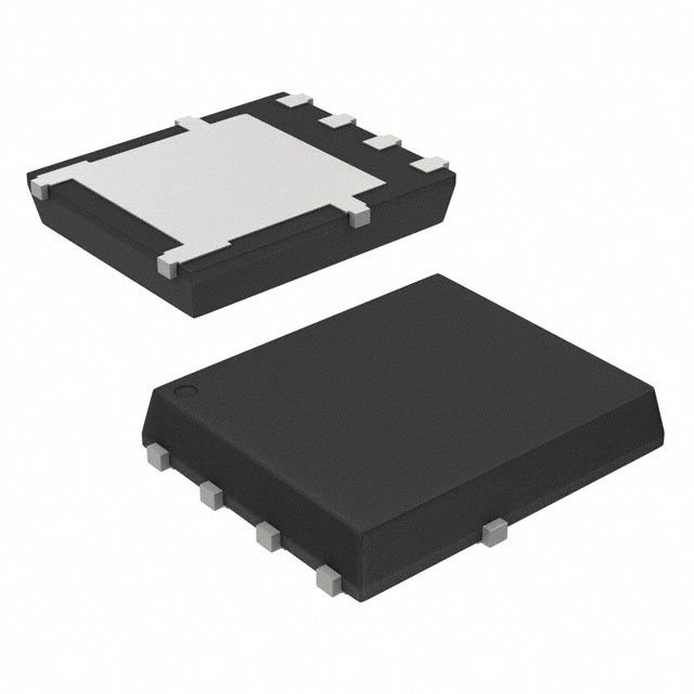
The NVMFS5C404NLWFAFT1G is a high-performance MOSFET N-CH 40V 370A 5DFN transistor designed and manufactured by onsemi. This device is specifically engineered for automotive applications, ensuring robust performance and reliability in demanding environments. With its advanced technology and unique features, the NVMFS5C404NLWFAFT1G stands out among similar models in the market.
NVMFS5C404NLWFAFT1G Features
- Input Capacitance (Ciss) (Max) @ Vds: 12168 pF @ 25 V
- Gate Charge (Qg) (Max) @ Vgs: 81 nC @ 4.5 V
- Drain to Source Voltage (Vdss): 40 V
- Power Dissipation (Max): 200W (Tc)
- Technology: MOSFET (Metal Oxide)
- REACH Status: REACH Unaffected
- Vgs (Max): ±20V
- RoHS Status: ROHS3 Compliant
- Moisture Sensitivity Level (MSL): 1 (Unlimited)
- Grade: Automotive
- Mounting Type: Surface Mount
- Rds On (Max) @ Id, Vgs: 0.67mOhm @ 50A, 10V
- Vgs(th) (Max) @ Id: 2V @ 250µA
- Current - Continuous Drain (Id) @ 25°C: 370A (Tc)
- Drive Voltage (Max Rds On, Min Rds On): 4.5V, 10V
NVMFS5C404NLWFAFT1G Applications
The NVMFS5C404NLWFAFT1G is ideal for a variety of applications where high power and performance are required. Some specific use cases include:
- Automotive Systems: Due to its automotive grade and robust design, this MOSFET is perfect for use in automotive powertrain, lighting, and control systems.
- Industrial Applications: The high power dissipation and drain current make it suitable for industrial motor drives and power supplies.
- Telecommunications: This device can be used in high-power telecommunications equipment, such as base stations and signal amplifiers.
Conclusion of NVMFS5C404NLWFAFT1G
The NVMFS5C404NLWFAFT1G is a powerful and reliable MOSFET designed for high-performance applications in the automotive and industrial sectors. Its unique features, such as low Rds On, high drain current, and advanced technology, make it a standout choice for demanding environments. With onsemi's commitment to quality and performance, the NVMFS5C404NLWFAFT1G is a trusted solution for your next high-power project.
FAQ
| Quantity | Unit Price | Ext. Price |
|---|---|---|
| 1+ | $6.97200 | $6.97 |
| 10+ | $6.68057 | $66.81 |
| 30+ | $6.50228 | $195.07 |
| 100+ | $6.35315 | $635.32 |
Not available to buy online? Want the lower wholesale price? Please Send RFQ to get best price, we will respond immediately


.png?x-oss-process=image/format,webp/resize,h_32)


